
Datasheet

LTC1871
16
1871fe
APPLICATIONS INFORMATION
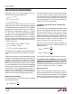
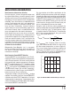
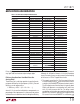
JUNCTION TEMPERATURE (°C)
–50
ρ
T
NORMALIZED ON RESISTANCE
1.0
1.5
150
1871 F11
0.5
0
0
50
100
2.0
Figure 11. Normalized R
DS(ON)
vs Temperature
Another method of choosing which power MOSFET to
use is to check what the maximum output current is for a
given R
DS(ON)
, since MOSFET on-resistances are available
in discrete values.
I
O(MAX)
= V
SENSE(MAX)
•
1–D
MAX
1+
2
•R
DS(ON)
•
T
It is worth noting that the 1 – D
MAX
relationship between
I
O(MAX)
and R
DS(ON)
can cause boost converters with a
wide input range to experience a dramatic range of maxi-
mum input and output current. This should be taken into
consideration in applications where it is important to limit
the maximum current drawn from the input supply.
Calculating Power MOSFET Switching and Conduction
Losses and Junction Temperatures
In order to calculate the junction temperature of the
power MOSFET, the power dissipated by the device must
be known. This power dissipation is a function of the
duty cycle, the load current and the junction temperature
itself (due to the positive temperature coeffi cient of its
R
DS(ON)
). As a result, some iterative calculation is normally
required to determine a reasonably accurate value. Since
the con
troller is using the MOSFET as both a switching
and a sensing element, care should be taken to ensure
that the converter is capable of delivering the required
load current over all operating conditions (line voltage
and temperature), and for the worst-case specifi cations
for V
SENSE(MAX)
and the R
DS(ON)
of the MOSFET listed in
the manufacturer’s data sheet.
The power dissipated by the MOSFET in a boost converter is:
P
FET
=
I
O(MAX)
1–D
MAX
2
•R
DS(ON)
•D
MAX
•
T
+k•V
O
1.85
•
I
O(MAX)
1–D
MAX
( )
•C
RSS
•f
The fi rst term in the equation above represents the I
2
R
losses in the device, and the second term, the switching
losses. The constant, k = 1.7, is an empirical factor inversely
related to the gate drive current and has the dimension
of 1/current.
From a known power dissipated in the power MOSFET, its
junction temperature can be obtained using the following
formula:
T
J
= T
A
+ P
FET
• R
TH(JA)
The R
TH(JA)
to be used in this equation normally includes
the R
TH(JC)
for the device plus the thermal resistance from
the case to the ambient temperature (R
TH(CA)
). This value
of T
J
can then be compared to the original, assumed value
used in the iterative calculation process.
Boost Converter: Output Diode Selection
To maximize effi ciency, a fast switching diode with low
forward drop and low reverse leakage is desired. The output
diode in a boost converter conducts current during the
switch off-time. The peak reverse voltage that the diode
must withstand is equal to the regulator output voltage.
The average forward current in normal operation is equal
to the output current, and the peak current is equal to the
peak inductor current.
I
D(PEAK)
= I
L(PEAK)
= 1+
2
•
I
O(MAX)
1–D
MAX
The power dissipated by the diode is:
P
D
= I
O(MAX)
• V
D
and the diode junction temperature is:
T
J
= T
A
+ P
D
• R
TH(JA)
The R
TH(JA)
to be used in this equation normally includes
the R
TH(JC)
for the device plus the thermal resistance from
the board to the ambient temperature in the enclosure.