
Datasheet
LTC1871
13
1871fe
APPLICATIONS INFORMATION
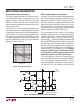
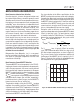
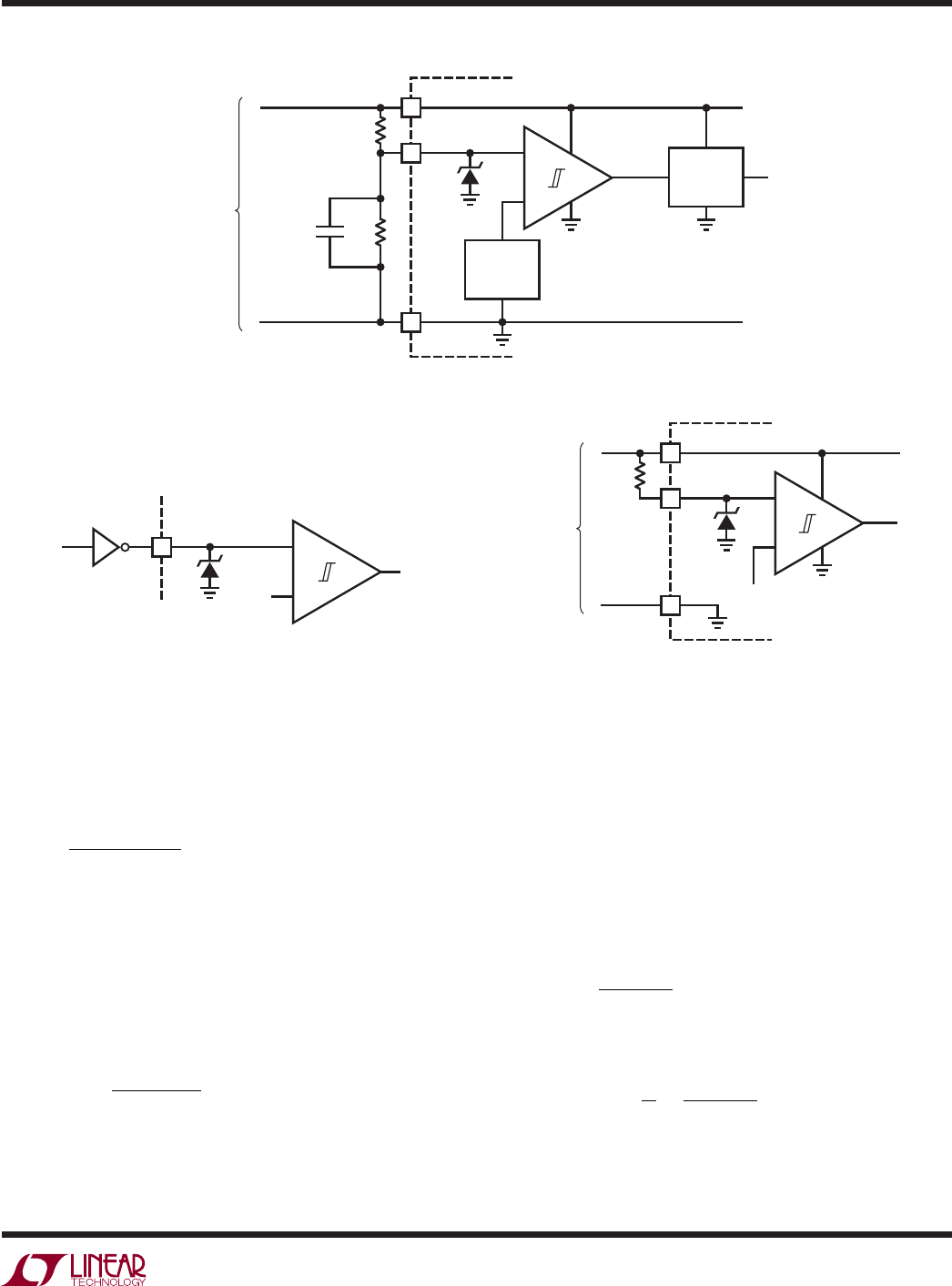
Figure 8a. Programming the Turn-On and Turn-Off Thresholds Using the RUN Pin
Boost Converter: Duty Cycle Considerations
For a boost converter operating in a continuous conduction
mode (CCM), the duty cycle of the main switch is:
D=
V
O
+ V
D
–V
IN
V
O
+ V
D
where V
D
is the forward voltage of the boost diode. For
converters where the input voltage is close to the output
voltage, the duty cycle is low and for converters that develop
a high output voltage from a low voltage input supply,
the duty cycle is high. The maximum output voltage for a
boost converter operating in CCM is:
V
O(MAX)
=
V
IN(MIN)
1–D
MAX
( )
–V
D
The maximum duty cycle capability of the LTC1871 is
typically 92%. This allows the user to obtain high output
voltages from low input supply voltages.
Boost Converter: The Peak and Average Input Currents
The control circuit in the LTC1871 is measuring the input
current (either by using the R
DS(ON)
of the power MOSFET
or by using a sense resistor in the MOSFET source), so
the output current needs to be refl ected back to the input
in order to dimension the power MOSFET properly. Based
on the fact that, ideally, the output power is equal to the
input power, the maximum average input current is:
I
IN(MAX)
=
I
O(MAX)
1–D
MAX
The peak input current is:
I
IN(PEAK)
= 1+
2
•
I
O(MAX)
1–D
MAX
The maximum duty cycle, D
MAX
, should be calculated at
minimum V
IN
.
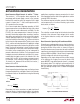
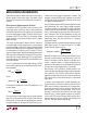
Figure 8c. External Pull-Up Resistor On
RUN Pin for “Always On” Operation
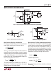
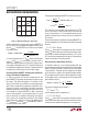
Figure 8b. On/Off Control Using External Logic
–
+
RUN
COMPARATOR
V
IN
RUN
R2
R1
INPUT
SUPPLY
OPTIONAL
FILTER
CAPACITOR
+
–
GND
1871 F8a
BIAS AND
START-UP
CONTROL
1.248V
µPOWER
REFERENCE
6V
–
+
RUN
COMPARATOR
1.248V
1871 F08b
RUN
6V
EXTERNAL
LOGIC CONTROL
–
+
RUN
COMPARATOR
V
IN
RUN
R2
1M
INPUT
SUPPLY
+
–
GND
1.248V
1871 F08c
6V