
Datasheet
LTC1871
11
1871fe
APPLICATIONS INFORMATION
Programming the Operating Frequency
The choice of operating frequency and inductor value is
a tradeoff between effi ciency and component size. Low
frequency operation improves effi ciency by reducing
MOSFET and diode switching losses. However, lower
frequency operation requires more inductance for a given
amount of load current.
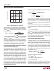
The LTC1871 uses a constant frequency architecture that
can be programmed over a 50kHz to 1000kHz range with
a single external resistor from the FREQ pin to ground, as
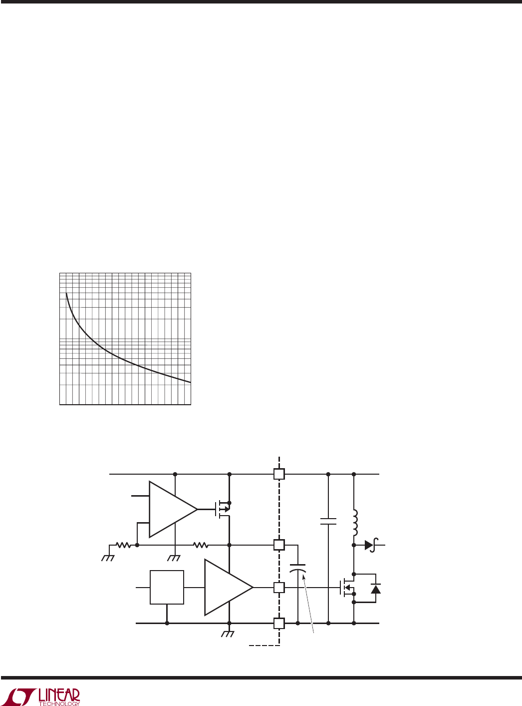
shown in Figure 1. The nominal voltage on the FREQ pin is
0.6V, and the current that fl ows into the FREQ pin is used
to charge and discharge an internal oscillator capacitor. A
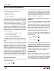
graph for selecting the value of R
T
for a given operating
frequency is shown in Figure 6.
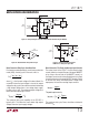
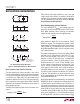
INTV
CC
Regulator Bypassing and Operation
An internal, P-channel low dropout voltage regulator pro-
duces the 5.2V supply which powers the gate driver and
logic circuitry within the LTC1871, as shown in Figure 7.
The INTV
CC
regulator can supply up to 50mA and must be
bypassed to ground immediately adjacent to the IC pins
with a minimum of 4.7µF tantalum or ceramic capacitor.
Good bypassing is necessary to supply the high transient
currents required by the MOSFET gate driver.
For input voltages that don’t exceed 7V (the absolute
maximum rating for this pin), the internal low dropout
regulator in the LTC1871 is redundant and the INTV
CC
pin
can be shorted directly to the V
IN
pin. With the INTV
CC
pin shorted to V
IN
, however, the divider that programs the
regulated INTV
CC
voltage will draw 10µA of current from
the input supply, even in shutdown mode. For applications
that require the lowest shutdown mode input supply cur-
rent, do not connect the INTV
CC
pin to V
IN
. Regardless of
whether the INTV
CC
pin is shorted to V
IN
or not, it is always
necessary to have the driver circuitry bypassed with a
4.7μF tantalum or low ESR ceramic capacitor to ground
immediately adjacent to the INTV
CC
and GND pins.
In an actual application, most of the IC supply current is
used to drive the gate capacitance of the power MOSFET.
As a result, high input voltage applications in which a
large power MOSFET is being driven at high frequencies
can cause the LTC1871 to exceed its maximum junction
Figure 6. Timing Resistor (R
T
) Value
FREQUENCY (kHz)
100
R
T
(kΩ)
300
1000
1871 F06
10
100
200 1000
900
800700600
500
400
0
Figure 7. Bypassing the LDO Regulator and Gate Driver Supply
+
–
+
1.230V
R2 R1
P-CH
5.2V
DRIVER
GATE
C
VCC
4.7µF
C
IN
INPUT
SUPPLY
2.5V TO 30V
GND
PLACE AS CLOSE AS
POSSIBLE TO DEVICE PINS
M1
1871 F07
INTV
CC
V
IN
GND
LOGIC