
Datasheet
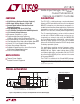
LTC1871
10
1871fe
MOSFET R
DS(ON)
. If the I
TH
pin drops below 0.30V, the
Burst Mode comparator B1 will turn off the power MOSFET
and scale back the quiescent current of the IC to 250µA
(sleep mode). In this condition, the load current will be
supplied by the output capacitor until the I
TH
voltage rises
above the 50mV hysteresis of the burst comparator. At
light loads, short bursts of switching (where the average
inductor current is 20% of its maximum value) followed
by long periods of sleep will be observed, thereby greatly
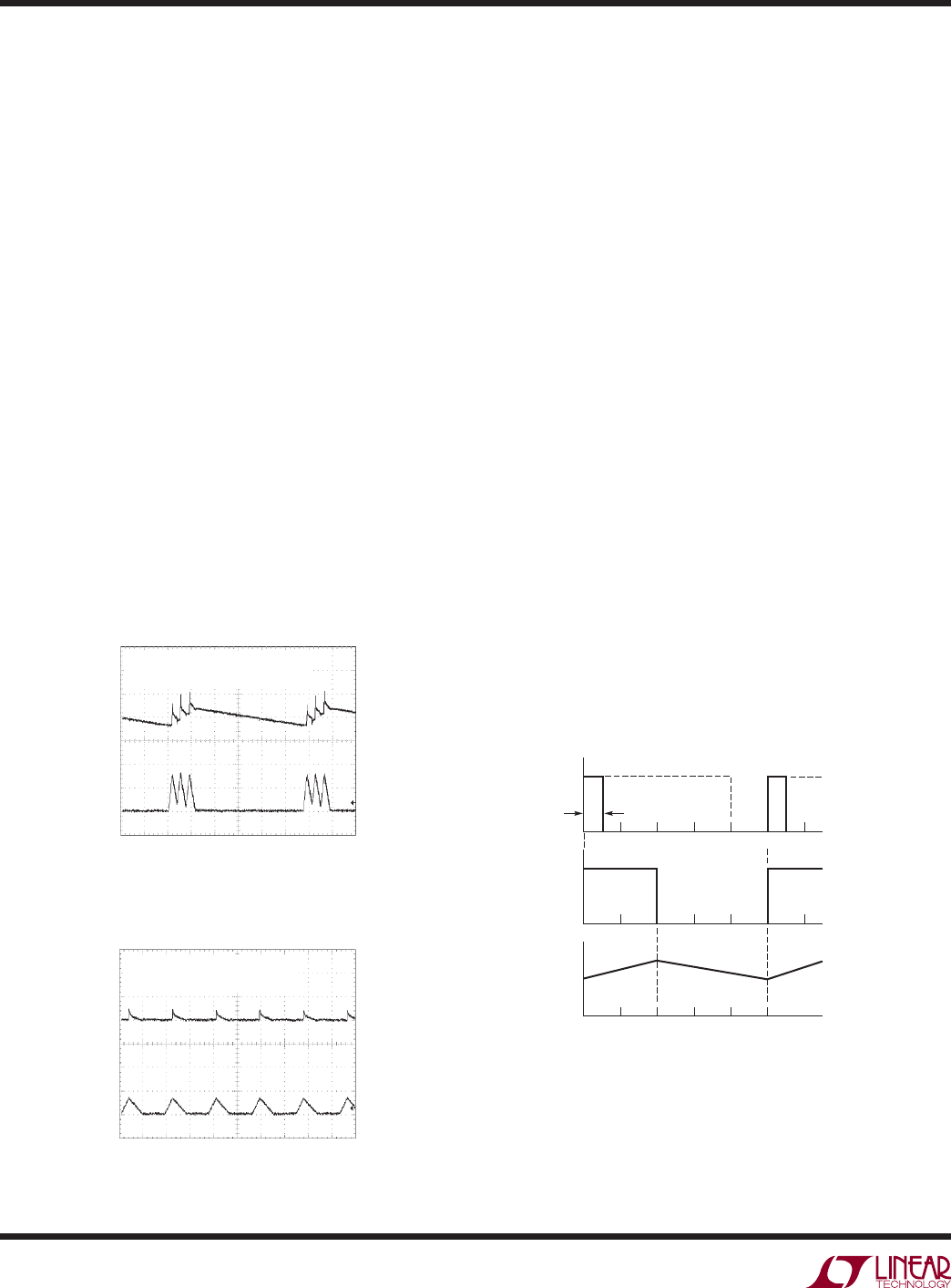
improving converter effi ciency. Oscilloscope waveforms
illustrating Burst Mode operation are shown in Figure 3.
Pulse-Skip Mode Operation
With the MODE/SYNC pin tied to a DC voltage above 2V,
Burst Mode operation is disabled. The internal, 0.525V
buffered I
TH
burst clamp is removed, allowing the I
TH
pin to directly control the current comparator from no
load to full load. With no load, the I
TH
pin is driven below
0.30V, the power MOSFET is turned off and sleep mode
is invoked. Oscilloscope waveforms illustrating this mode
of operation are shown in Figure 4.
When an external clock signal drives the MODE/SYNC
pin at a rate faster than the chip’s internal oscillator, the
oscillator will synchronize to it. In this synchronized mode,
Burst Mode operation is disabled. The constant frequency
associated with synchronized operation provides a more
controlled noise spectrum from the converter, at the ex-
pense of overall system effi ciency of light loads.
When the oscillator’s internal logic circuitry detects a
synchronizing signal on the MODE/SYNC pin, the in-
ternal oscillator ramp is terminated early and the slope
compensation is increased by approximately 30%. As
a result, in applications requiring synchronization, it is
recommended that the nominal operating frequency of
the IC be programmed to be about 75% of the external
clock frequency. Attempting to synchronize to too high an
external frequency (above 1.3f
O
) can result in inadequate
slope compensation and possible subharmonic oscillation
(or jitter).
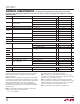
The external clock signal must exceed 2V for at least 25ns,
and should have a maximum duty cycle of 80%, as shown
in Figure 5. The MOSFET turn on will synchronize to the
rising edge of the external clock signal.
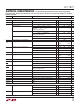
Figure 3. LTC1871 Burst Mode Operation
(MODE/SYNC = 0V) at Low Output Current
Figure 4. LTC1871 Low Output Current Operation with
Burst Mode Operation Disabled (MODE/SYNC = INTV
CC
)
V
OUT
50mV/DIV
I
L
5A/DIV
10µs/DIV
1871 F03
V
IN
= 3.3V
V
OUT
= 5V
I
OUT
= 500mA
MODE/SYNC = 0V
(Burst Mode OPERATION)
V
OUT
50mV/DIV
I
L
5A/DIV
2µs/DIV
1871 F04
V
IN
= 3.3V
V
OUT
= 5V
I
OUT
= 500mA
MODE/SYNC = INTV
CC
(PULSE-SKIP MODE)
OPERATION
Figure 5. MODE/SYNC Clock Input and Switching
Waveforms for Synchronized Operation
1871 F05
2V TO 7V
MODE/
SYNC
GATE
I
L
t
MIN
= 25ns
0.8T
D = 40%
T T = 1/f
O