
Datasheet


5
LTC1257
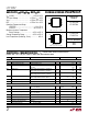
TYPICAL PERFORMANCE CHARACTERISTICS
UW
C
L
(µF)
0.01
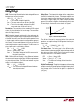
REFERENCE COMPENSATION RESISTANCE (Ω)
70
60
50
40
30
20
10
0
0.1 1
1257 G11
10 100
Reference Compensation
Resistance vs C
L
Broadband Noise
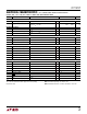
PI FU CTIO S
U
UU
GND (Pin 5): Ground.
REF (Pin 6): The output of the 2.048V reference and the
input to the DAC resistor ladder. An external reference with
voltage from 2.475V to V
CC
– 2.7V may be used to override
the internal reference.
V
OUT
(Pin 7): The buffered DAC output is capable of
sourcing 2mA over temperature while pulling within 2.7V
of V
CC
. The output will pull to ground through an internal
200Ω equivalent resistance.
V
CC
(Pin 8): The positive supply input. 4.75V ≤ V
CC
≤
15.75V. Requires a bypass capacitor to ground.
CLK (Pin 1): The TTL level input for the serial interface
clock.
D
IN
(Pin 2): The TTL level input for the serial interface data.
Data on the D
IN
pin is latched into the shift register on the
rising edge of the serial clock.
LOAD (Pin 3): The TTL level input for the serial interface
load control. Data is loaded from the shift register into the
DAC register, thus updating the DAC output when LOAD is
pulled low. The DAC register is transparent as long as
LOAD is held low.
D
OUT
(Pin 4): The output of the shift register which
becomes valid on the rising edge of the serial clock. The
D
OUT
pin is driven from GND to V
CC
by an internal CMOS
inverter. Multiple LTC1257s may be cascaded by connect-
ing the D
OUT
pin to the D
IN
pin of the next chip.
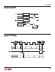
CODE
0
DNL ERROR (LSBs)
0.5
0.0
–0.5
1024 2048 2560
1257 TA05
512 1536 3072 3584
4098
Differential Nonlinearity (DNL)
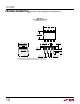
TIME = 5ms/DIV
0.1V/DIV
1257 G12
CODE = FFFH
BW = 3Hz TO 1MHz
GAIN = 1100×