
Datasheet


9
LTC1090
1090fc
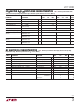
TYPICAL PERFOR A CE CHARACTERISTICS
UW
Digital Input Logic Threshold vs
Supply Voltage
Input Channel Leakage Current
vs Temperature Noise Error vs Reference Voltage
The LTC1090 is a data acquisition component which
contains the following functional blocks:
1. 10-bit successive approximation capacitive
A/D converter
2. Analog multiplexer (MUX)
3. Sample and hold (S/H)
4. Synchronous, full duplex serial interface
5. Control and timing logic
DIGITAL CONSIDERATIONS
1. Serial Interface
The LTC1090 communicates with microprocessors and
other external circuitry via a synchronous, full duplex,
four wire serial interface (see Operating Sequence). The
shift clock (SCLK) synchronizes the data transfer with
each bit being transmitted on the falling SCLK edge
and captured on the rising SCLK edge in both transmit-
ting and receiving systems. The data is transmitted and
received simultaneously (full duplex).
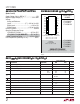
Operating Sequence
(Example: Differential Inputs (CH3 to CH2), Bipolar, MSB First and 10-Bit Word Length)
REFERENCE VOLTAGE, V
REF
(V)
0.2
PEAK-TO-PEAK NOISE ERROR (LSBs)
0.5
1.0
2.0
15
LTC1090 • TPC21
1.5
0.25
0.75
1.75
1.25
LTC1090 NOISE = 200µV PEAK-TO-PEAK
APPLICATIO S I FOR ATIO
WUUU
SUPPLY VOLTAGE, V
CC
(V)
4
0
LOGIC THRESHOLD (V)
1
2
3
4
5678
LTC1090 • TPC19
910
T
A
= 25°C
AMBIENT TEMPERATURE, T
A
(°C)
–50
INPUT CHANNEL LEAKAGE CURRENT (nA)
100
300
400
500
1000
700
0
50
75
LTC1090 • TPC20
200
800
900
600
–25
25
100
125
GUARANTEED
ON CHANNEL
OFF CHANNELS
LTC1090 • AI01
B9
(SB)
SHIFT A/D RESULT OUT AND
NEW CONFIGURATION WORD IN
B8 B7 B6 B5 B4 B3 B2 B1 B0
SHIFT CONFIGURATION
WORD IN
ODD/
SIGN
SGL/
DIFF
SEL1
D
IN
CS
15810
SCLK
D
OUT
SEL0 UNI
MSBF
WL1 WL0
t
CYC
t
SMPL
t
CONV
DON’T CARE
DON’T CARE