
Datasheet


15
LTC1090
1090fc
serial formats (see Table 2). If an MPU without a serial
interface is used, then 4 of the MPU’s parallel port lines can
be programmed to form the serial link to the LTC1090.
Included here are three serial interface examples and one
example showing a parallel port programmed to form the
serial interface.
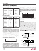
Table 2. Microprocessors with Hardware Serial Interfaces
Compatible with the LTC1090**
PART NUMBER TYPE OF INTERFACE
Motorola
MC6805S2, S3 SPI
MC68HC11 SPI
MC68HC05 SPI
RCA
CDP68HC05 SPI
Hitachi
HD6305 SCI Synchronous
HD63705 SCI Synchronous
HD6301 SCI Synchronous
HD63701 SCI Synchronous
HD6303 SCI Synchronous
National Semiconductor
COP400 Family MICROWIRE
†
COP800 Family MICROWIRE/PLUS
†
NS8050U MICROWIRE/PLUS
HPC16000 Family MICROWIRE/PLUS
Texas Instruments
TMS7002 Serial Port
TMS7042 Serial Port
TMS70C02 Serial Port
TMS70C42 Serial Port
TMS32011* Serial Port
TMS32020* Serial Port
*Requires external hardware
**Contact LTC Marketing for interface information for processors not on
this list
†
MICROWIRE and MlCROWIRE/PLUS are trademarks of National
Semiconductor Corp.
Serial Port Microprocessors
Most synchronous serial formats contain a shift clock
(SCLK) and two data lines, one for transmitting and one for
receiving. In most cases data bits are transmitted on the
falling edge of the clock (SCLK) and captured on the rising
edge. However, serial port formats vary among MPU
manufacturers as to the smallest number of bits that can
be sent in one group (e.g., 4-bit, 8-bit or 16-bit transfers).
They also vary as to the order in which the bits are
transmitted (LSB or MSB first). The following examples
show how the LTC1090 accommodates these differences.
National MICROWIRE (COP420)
The COP420 transfers data MSB first and in 4-bit incre-
ments (nibbles). This is easily accommodated by setting
the LTC1090 to MSB first format and 12-bit word length.
The data output word is then received by the COP420 in
three 4-bit blocks with the final two unused bits filled with
zeroes by the LTC1090.
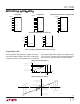
Hardware and Software Interface to National Semiconductor
COP420 Processor
APPLICATIO S I FOR ATIO
WUUU
MNEMONIC DESCRIPTION
LEI Enable SlO
SC Set Carry flag
OGI G0 is set to (CS goes low)
LDD Load first 4 bits of D
IN
to ACC
XAS Swap ACC with SIO reg. Starts SK Clk
LDD Load 2nd 4 bits of D
IN
to ACC
NOP Timing
XAS Swap first 4 bits from A/D with ACC. SK continues.
XIS Put first 4 bits in RAM (location A)
NOP Timing
XAS Swap 2nd 4 bits from A/D with ACC. SK continues.
XIS Put 2nd 4 bits in RAM (location A + 1)
RC Clear Carry
NOP Timing
XAS Swap 3rd 4 bits from A/D with ACC. SK off
XIS Put 3rd 4 bits in RAM (location A + 2)
OGI G0 is set to 1 (CS goes high)
LEI Disable SlO
LTC1090
ANALOG
INPUTS
D
OUT
D
OUT
from LTC1090 stored in COP420 RAM
D
IN
SCLK
GO
SK
SO
SI
COP420
CS
B9
Location A
Location A + 1
first 4 bits
second 4 bits
third 4 bits
LSB
MSB*
B8 B7 B6
B5 B4 B3 B2
Location A + 2
B1 B0 B0 B0
LTC1090 • AI11
*B9 is MSB in unipolar or sign bit in bipolar