
Datasheet


12
LTC1090
1090fc
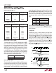
Unipolar Output Code (UNI = 1)
INPUT VOLTAGE
OUTPUT CODE INPUT VOLTAGE (V
REF
= 5V)
1111111111 V
REF
– 1LSB 4.9951V
1111111110 V
REF
– 2LSB 4.9902V
•••
•••
•••
0000000001 1LSB 0.0049V
0000000000 0V 0V
Bipolar Output Code (UNI = 0)
INPUT VOLTAGE
OUTPUT CODE INPUT VOLTAGE (V
REF
= 5V)
0111111111 V
REF
– 1LSB 4.9902V
0111111110 V
REF
– 2LSB 4.9805V
•••
•••
•••
0000000001 1LSB 0.0098V
0000000000 0V 0V
1111111111 –1LSB –0.0098V
1111111110 –2LSB –0.0195V
•••
•••
•••
1000000001 – (V
REF
) + 1LSB –4.9902V
1000000000 – (V
REF
)–5.000V
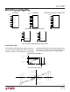
MSB First/LSB First Format (MSBF)
The output data of the LTC1090 is programmed for MSB
first or LSB first sequence using the MSBF bit. For MSB
first output data the input word clocked to the LTC1090
should always contain a logical one in the sixth bit location
(MSBF bit). Likewise for LSB first output data, the input
word clocked to the LTC1090 should always contain a zero
in the MSBF bit location. The MSBF bit in a given D
IN
word
will control the order of the next D
OUT
word. The MSBF bit
affects only the order of the output data word. The order
of the input word is unaffected by this bit.
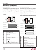
MSBF OUTPUT FORMAT
0LSB First
1 MSB First
Word Length (WL1, WL0)
The last two bits of the input word (WL1 and WL0) program
the output data word length of the LTC1090. Word lengths
of 8, 10, 12 or 16 bits can be selected according to the
following table. The WL1 and WL0 bits in a given D
IN
word
control the length of the present, not the next, D
OUT
word.
WL1 and WL0 are never “don’t cares” and must be set for
the correct D
OUT
word length even when a “dummy” D
IN
word is sent. On any transfer cycle, the word length should
be made equal to the number of SCLK cycles sent by the
MPU.
WL1 WL0 OUTPUT WORD LENGTH
00 8 Bits
01 10 Bits
10 12 Bits
11 16 Bits
Figure 2 shows how the data output (D
OUT
) timing can be
controlled with word length selection and MSB/LSB first
format selection.
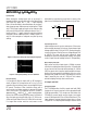
3. Deglitcher
A deglitching circuit has been added to the Chip Select
input of the LTC1090 to minimize the effects of errors
caused by noise on that input. This circuit ignores changes
in state on the CS input that are shorter in duration than 1
ACLK cycle. After a change of state on the CS input, the
LTC1090 waits for two falling edges of the ACLK before
recognizing a valid chip select. One indication of CS low
recognition is the D
OUT
line becoming active (leaving the
Hi-Z state). Note that the deglitching applies to both the
rising and falling CS edges.
APPLICATIO S I FOR ATIO
WUUU
HIGH Z
HIGH Z
ACLK
ACLK
VALID OUTPUT
D
OUT
D
OUT
CS
CS
LOW CS RECOGNIZED
INTERNALLY
HIGH CS RECOGNIZED
INTERNALLY
LTC1090 • AI07