
Datasheet


8
LT3503
3503f
APPLICATIO S I FOR ATIO
WUU
U
FB Resistor Network
The output voltage is programmed with a resistor divider
between the output and the FB pin. Choose the 1%
resistors according to:
RR
V
V
OUT
12
078
1=
⎛
⎝
⎜
⎞
⎠
⎟
.
–
R2 should be 20.0k or less to avoid bias current errors.
Reference designators refer to the Block Diagram.
An optional phase lead capacitor of 22pF between V
OUT
and FB reduces light-load output ripple.
Input Voltage Range
The input voltage range for LT3503 applications depends
on the output voltage and on the absolute maximum
ratings of the V
IN
and BOOST pins.
The minimum input voltage is determined by either the
LT3503’s minimum operating voltage of 3.6V, or by its
maximum duty cycle. The duty cycle is the fraction of time
that the internal switch is on and is determined by the input
and output voltages:
DC
VV
VV V
OUT D
IN SW D
=
+
+–
where V
D
is the forward voltage drop of the catch diode
(~0.4V) and V
SW
is the voltage drop of the internal switch
(~0.4V at maximum load). This leads to a minimum input
voltage of:
V
VV
DC
VV
IN MIN
OUT
D
MAX
D
SW
()
–=
+
+
with DC
MAX
= 0.81 (0.76 over temperature).
The maximum input voltage is determined by the absolute
maximum ratings of the V
IN
and BOOST pins. For con-
stant-frequency operation the maximum input voltage is
determined by the minimum duty cycle, DC
MIN
= 0.29. If
the duty cycle requirement is less than DC
MIN
, the part will
enter pulse-skipping mode. The onset of pulse-skipping
occurs at:
V
VV
DC
VV
IN PS
OUT
D
MIN
D
SW()
–=
+
+
In pulse-skipping mode the part skips pulses to control the
inductor current and regulate the output voltage, possibly
producing a spectrum of frequencies below 2.2MHz.
Note that this is a restriction on the operating input voltage
to remain in constant-frequency operation; the circuit will
tolerate transient inputs up to the absolute maximum
ratings of the V
IN
and BOOST pins when the output is in
regulation. The input voltage should be limited to V
IN(PS)
during overload conditions (short-circuit or start-up).
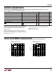
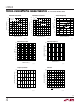
Minimum On Time
The part will still regulate the output at input voltages that
exceed V
IN(PS)
(up to 20V), but the output voltage ripple
increases. Figure 1 illustrates switching waveforms in
continuous mode for a 0.78V output application near
V
IN(PS)
= 6V.
As the input voltage is increased, the part is required to
switch for shorter periods of time. Delays associated with
turning off the power switch dictate the minimum on time
of the part. The minimum on time for the LT3503 is
~130ns. Figure 2 illustrates the switching waveforms
when the input voltage is increased to V
IN
= 14V.
Figure 1
Figure 2
V
SW
10V/DIV
V
OUT
20mV/DIV
C
OUT
= 47µF
V
OUT
= 0.78V
V
IN
= 7V
I
LOAD
= 1.1A
L = 1.1µH
1µs/DIV
3503 F01
I
L
1A/DIV
V
SW
10V/DIV
V
OUT
20mV/DIV
C
OUT
= 47µF
V
OUT
= 0.78V
V
IN
= 14V
I
LOAD
= 1.1A
L = 1.1µH
1µs/DIV
3503 F02
I
L
1A/DIV