
Datasheet
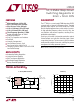


3
LT3503
3503f
PARAMETER CONDITIONS MIN TYP MAX UNITS
Switch Current Limit (Note 3) 1.45 1.75 2.2 A
Switch V
CESAT
I
SW
= 1A 400 mV
Switch Leakage Current 2 µA
Minimum Boost Voltage Above Switch I
SW
= 1A 2 2.3 V
BOOST Pin Current I
SW
= 1A 25 50 mA
SHDN Input Voltage High 2.3 V
SHDN Input Voltage Low 0.3 V
SHDN Bias Current V
SHDN
= 2.3V (Note 5) 6 15 µA
V
SHDN
= 0V 0.01 0.1 µA
The ● denotes specifications which apply over the full operating temperature range, otherwise specifications are at T
A
= 25°C.
V
IN
= 12V, V
BOOST
= 17V, unless otherwise noted. (Note 2)
ELECTRICAL CHARACTERISTICS
Note 1: Stresses beyond those listed under Absolute Maximum Ratings
may cause permanent damage to the device. Exposure to any Absolute
Maximum Rating condition for extended periods may affect device
reliability and lifetime.
Note 2: The LT3503E is guaranteed to meet performance specifications
from 0°C to 85°C. Specifications over the –40°C to 85°C operating
temperature range are assured by design, characterization and correlation
with statistical process controls.
Note 3: Current limit guaranteed by design and/or correlation to static test.
Slope compensation reduces current limit at higher duty cycle.
Note 4: Current flows out of pin.
Note 5: Current flows into pin.
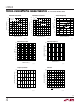
TYPICAL PERFOR A CE CHARACTERISTICS
UW
Efficiency (V
OUT
= 3.3V)
Efficiency (V
OUT
= 5V)
T
A
= 25°C unless otherwise noted.
LOAD CURRENT (A)
0
EFFICIENCY (%)
82
86
90
0.8
3503 G01
78
74
80
84
88
76
72
70
0.2
0.4
0.6
1.0
1.2
V
IN
= 8V
L = 2.5µH
V
IN
= 12V
LOAD CURRENT (A)
0
EFFICIENCY (%)
82
86
90
0.8
3503 G02
78
74
80
84
88
76
72
70
0.2
0.4
0.6
1.0
1.2
V
IN
= 12V
L = 3.3µH
V
IN
= 16V