
Datasheet

LT3468/LT3468-1/LT3468-2
9
346812fa
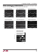
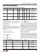
Table 2. Pre-Designed Transformers - Typical Specifications Unless Otherwise Noted.
SIZE L
PRI LPRI-LEAKAGE
R
PRI
R
SEC
FOR USE WITH TRANSFORMER NAME (W × L × H) mm (µH) (nH) N (mΩ)(Ω) VENDOR
LT3468/LT3468-2 SBL-5.6-1 5.6 × 8.5 × 4.0 10 200 Max 10.2 103 26 Kijima Musen
LT3468-1 SBL-5.6S-1 5.6 × 8.5 × 3.0 24 400 Max 10.2 305 55 Hong Kong Office
852-2489-8266 (ph)
kijimahk@netvigator.com (email)
LT3468 LDT565630T-001 5.8 × 5.8 × 3.0 6 200 Max 10.4 100 Max 10 Max TDK
LT3468-1 LDT565630T-002 5.8 × 5.8 × 3.0 14.5 500 Max 10.2 240 Max 16.5 Max Chicago Sales Office
LT3468-2 LDT565630T-003 5.8 × 5.8 × 3.0 10.5 550 Max 10.2 210 Max 14 Max (847) 803-6100 (ph)
www.components.tdk.com
LT3468/LT3468-1 T-15-089 6.4 × 7.7 × 4.0 12 400 Max 10.2 211 Max 27 Max Tokyo Coil Engineering
LT3468-1 T-15-083 8.0 × 8.9 × 2.0 20 500 Max 10.2 675 Max 35 Max Japan Office
0426-56-6262 (ph)
www.tokyo-coil.co.jp
Capacitor Selection
For the input bypass capacitor, a high quality X5R or X7R
type should be used. Make sure the voltage capability of
the part is adequate.
Output Diode Selection
The rectifying diode(s) should be low capacitance type
with sufficient reverse voltage and forward current rat-
ings. The peak reverse voltage that the diode(s) will see is
approximately:
VVNV
PK R OUT IN−
=+
()
•
The peak current of the diode is simply:
I
N
PK SEC−
=
14.
(LT3468)
I
N
PK SEC−
=
10.
(LT3468-2)
I
N
PK SEC−
=
07.
(LT3468-1)
For the circuit of Figure 6 with V
IN
of 5V, V
PK-R
is 371V and
I
PK-SEC
is 137mA. The GSD2004S dual silicon diode is
recommended for most LT3468/LT3468-1/LT3468-2
applications. Another option is to use the BAV23S dual
silicon diodes. Diodes Incorporated makes a dual diode
named MMBD3004S which also meets all the require-
ments. Table 3 shows the various diodes and relevant
specifications. Use the appropriate number of diodes to
achieve the necessary reverse breakdown voltage.
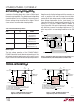
SW Pin Clamp Diode Selection
The diode D2 in Figure 6 is needed to clamp the SW node.
Due to the new control scheme of the LT3468/LT3468-1/
LT3468-2, the SW node may go below ground during a
switch cycle. The clamp diode prevents the SW node from
going too far below ground. The diode is required for
proper operation of the circuit. The recommended diode
Table 3. Recommended Output Diodes
MAX REVERSE VOLTAGE MAX FORWARD CONTINUOUS CURRENT CAPACITANCE
PART (V) (mA) (pF) VENDOR
GSD2004S 2x300 225 5 Vishay
(Dual Diode) (402) 563-6866
www.vishay.com
BAV23S 2x250 225 5 Philips Semiconductor
(Dual Diode) (800) 234-7381
www.philips.com
MMBD3004S 2x350 225 5 Diodes Incorporated
(805) 446-4800
www.diodes.com
APPLICATIO S I FOR ATIO
WUU
U