
Datasheet

LT3468/LT3468-1/LT3468-2
8
346812fa
Where: V
OUT
is the desired output voltage. The number
2 in the numerator is used to include the effect of the
voltage drop across the output diode(s).
Thus for a 320V output, N should be 322/31.5 or 10.2.
For a 300V output, choose N equal to 302/31.5 or 9.6.
The next parameter that needs to be set is the primary
inductance, L
PRI
. Choose L
PRI
according to the following
formula:
L
V
NI
PRI
OUT
PK
≥
−
••
•
200 10
9
Where: V
OUT
is the desired output voltage. N is
the transformer turns ratio. I
PK
is 1.4 (LT3468), 0.7
(LT3468-1), and 1.0 (LT3468-2).
L
PRI
needs to be equal or larger than this value to ensure
that the LT3468/LT3468-1/LT3468-2 has adequate time
to respond to the flyback waveform.
All other parameters need to meet or exceed the recom-
mended limits as shown in Table 1. A particularly impor-
tant parameter is the leakage inductance, L
LEAK
. When the
power switch of the LT3468/LT3468-1/LT3468-2 turns
off, the leakage inductance on the primary of the trans-
former causes a voltage spike to occur on the SW pin. The
height of this spike must not exceed 40V, even though the
absolute maximum rating of the SW Pin is 50V. The 50V
absolute maximum rating is a DC blocking voltage speci-
fication, which assumes that the current in the power NPN
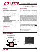
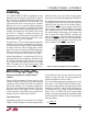
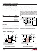
is zero. Figure 3 shows the SW voltage waveform for the
circuit of Figure 6(LT3468). Note that the absolute maxi-
mum rating of the SW pin is not exceeded. Make sure to
check the SW voltage waveform with V
OUT
near the target
output voltage, as this is the worst case condition for SW
voltage. Figure 4 shows the various limits on the SW
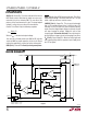
voltage during switch turn off.
It is important not to minimize the leakage inductance to
a very low level. Although this would result in a very low
leakage spike on the SW pin, the parasitic capacitance of
the transformer would become large. This will adversely
effect the charge time of the photoflash circuit.
Linear Technology has worked with several leading mag-
netic component manufacturers to produce pre-designed
flyback transformers for use with the LT3468/LT3468-1/
LT3468-2. Table 2 shows the details of several of these
transformers.
APPLICATIO S I FOR ATIO
WUU
U
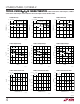
Figure 4. New Transformer Design Check (Not to Scale).
Figure 3. LT3468 SW Voltage Waveform
V
IN
= 5V
V
OUT
= 320V
3468 G18
100ns/DIV
V
SW
10V/DIV
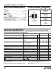
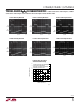
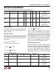
Table 1. Recommended Transformer Parameters
TYPICAL RANGE TYPICAL RANGE TYPICAL RANGE
PARAMETER NAME LT3468 LT3468-1 LT3468-2 UNITS
L
PRI
Primary Inductance >5 >10 >7 µH
L
LEAK
Primary Leakage Inductance 100 to 300 200 to 500 200 to 500 nH
N Secondary: Primary Turns Ratio 8 to 12 8 to 12 8 to 12
V
ISO
Secondary to Primary Isolation Voltage >500 >500 >500 V
I
SAT
Primary Saturation Current >1.6 >0.8 >1.0 A
R
PRI
Primary Winding Resistance <300 <500 <400 mΩ
R
SEC
Secondary Winding Resistance <40 <80 <60 Ω
V
SW
3420 F07
0V
“A”
“B”
MUST BE
LESS THAN 40V
MUST BE
LESS THAN 50V