
User's Manual
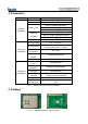
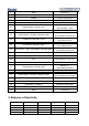
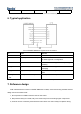
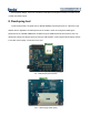
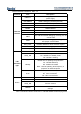
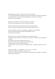
Table Of Contents

RX current 50 mA
Table1-2 LSD4WF-2MD05101 behavior of electricity
6. Typical application
Pic1-5 LSD4WF-2MD05101 Typical circuit connection
Pin State Remark
NRST411 Input, valid in low level Module reset pin with internal pull resistor
nlink Output (connected to LED) Check the network state of module or indication
for batch upgrade or configuration
nReload Input, valid in low level Connect button to chip pin for factory setting
restoring
Sleep_RQ Input, standby control Connect button to chip pin for module dormancy
managing
Sleep_ON Output, standby state indication Indication of dormancy state, connected with
LED
USART_TX/USAR
T_RX
Serial port transceiver port Serial port transceiver port
Table 1-3 Connection introduction of cardinal pin
7. Reference design
PCB onboard antenna is built in LSD4WF-2MD05101 module, users should using onboard antenna
design need to be cautious that:
1, No components or GND on antenna area of user board
2, Keep antenna away from metal, stay over 10mm away from surrounding higher components.
3, Antenna can’t be covered by metal case and it should be over 10mm away from plastic casing.