
Users Manual Part 1
Page 9 of 21
*The dimensional tolerances not shown in the figure are in accordance with the GB/T1804-m
standard.
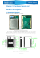
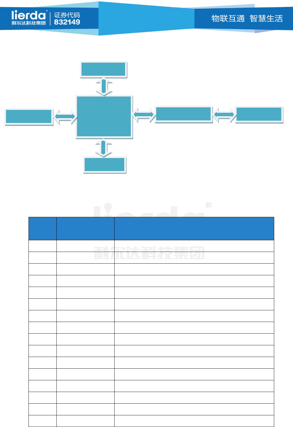
Figure 3-3 Internal block diagram of the S95 series module.
3.2Dimensionaldrawing
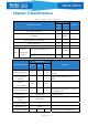
Table 3-1 Module Pin Function Description
Module
Pin
Chip
Pin
Remarks
1 P0.05 Digital I/O Pin
2 P0.12 Digital I/O Pin
3 P0.14 Digital I/O Pin
4 SWDIO Debug Data Pin
5 GND Power Ground
6 SWDCLK Debug Clock Pin
7 P0.20 Digital I/O Pin
8 P0.16 Digital I/O Pin
9 VCC Power Supply
10 GND Power Ground
11 RESET Reset Pin
12 P0.18 Digital I/O Pin ;
13 P0.04 Digital I/O Pin ;
14 P0.01 Digital I/O Pin ;
15 P0.00 Digital I/O Pin ;
16 GND Power Ground
nRF52x
32MHz
Filter Circuit
IO
ANT
POWER