
Datasheet

Page 1/3
110214/10 LEM reserves the right to carry out modications on its transducers, in order to improve them, without prior notice www.lem.com
Current Transducer LTSR 25-NP
For the electronic measurement of currents: DC, AC, pulsed, mixed,
with galvanic isolation between the primary circuit (high power) and
the secondary circuit (electronic circuit).
Electrical data
I
PN
Primary nominal current rms 25 At
I
PM
Primary current, measuring range 0 .. ± 80
1)
At
Î
P
Overload capability 250 At
V
OUT
Output voltage (Analog) @ I
P
2.5
±
(0.625·I
P
/I
PN
) V
I
P
= 0 2.5
2)
V
V
REF
Reference voltage (internal reference), Ref
OUT
mode 2.5
3)
V
Reference voltage (external reference), Ref
IN
mode 1.9 .. 2.7
4)
V
G Sensitivity 25 mV/A
N
S
Number of secondary turns (± 0.1 %) 2000
R
L
Load resistance ≥ 2 kW
C
L max
Maximum capacitive loading 500 pF
R
IM
Internal measuring resistance (± 0.5 %) 50 W
TCR
IM
Temperature coefcient of R
IM
< 50 ppm/K
V
C
Supply voltage (± 5 %) 5 V
I
C
Current consumption @ V
C
= 5 V Typ 28+I
S
5)
+(V
OUT
R/
L
) mA
Accuracy - Dynamic performance data
X Accuracy @ I
PN
, T
A
= 25°C ± 0.2 %
Accuracy with R
IM
@ I
PN
, T
A
= 25°C ± 0.7 %
e
L
Linearity error < 0.1 %
Max
TCV
OUT
Temperature coefcient of V
OUT
/V
REF
@ I
P
= 0
- 40°C .. + 85°C 37.5 ppm/K
TCG
Temperature coefcient of G - 40°C .. + 85°C 50
6)
ppm/K
V
OM
Magnetic offset voltage
@ I
P
= 0,
after an overload of 3 x I
PN
± 0.5 mV
5 x I
PN
± 2.0 mV
10 x I
PN
± 2.0 mV
TCV
REF
Temperature coefcient of internal V
REF
@ I
P
= 0 - 10°C .. + 85°C 50 ppm/K
- 40°C .. - 10°C 100 ppm/K
t
ra
Reaction time @ 10 % of I
PN
< 100 ns
t
r
Response time to 90 % of I
PN
step < 400 ns
di/dt di/dt accurately followed > 60 A/µs
BW Frequency bandwidth (0 .. - 0.5 dB) DC .. 100 kHz
(- 0.5 .. 1 dB) DC .. 200 kHz
Notes:
1)
Only in ref
OUT
mode or with external REF less than 2.525 V and greater than
2.475 V. For external REF out of these limits see leaet.
2)
V
OUT
is
linked to V
REF
, by
conception the difference between these two nodes for I
P
= 0 is maximum ± 25 mV,
2.475 V < V
OUT
< 2.525 V.
3)
In Ref
OUT
mode at T
A
= 25°C, 2.475 V< V
REF
< 2.525 V. The minimal impedance loading the ref pin should be > 220 kW. Internal
impedance = 600 W. For most applications you need to buffer this output to feed it
into an ADC for example.
4)
To overdrive the REF (1.9 V .. 2.7 V) max ± 1 mA is
needed.
5)
I
S
= I
P
/N
S
.
6)
Only due to TCR
IM
.
Features
● Closed loop (compensated)
multirange current transducer
using the Hall effect
● Unipolar voltage supply
● Isolated plastic case recognized
according to UL 94-V0
● Compact design for PCB
mounting
● Incorporated measuring
resistance
● Extended measuring range
● Access to the internal voltage
reference
● Possibility to feed the transducer
reference from external supply.
Advantages
● Excellent accuracy
● Very good linearity
● Very low temperature drift
● Optimized response time
● Wide frequency bandwidth
● No insertion losses
● High immunity to external
interference
● Current overload capability.
Applications
● AC variable speed drives and
servo motor drives
● Static converters for DC motor
drives
● Battery supplied applications
● Uninterruptible Power Supplies (UPS)
● Switched Mode Power Supplies
(SMPS)
● Power supplies for welding
applications.
Application Domain
● Industrial.
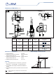
16171
I
PN
= 25 At