
User Manual
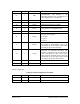
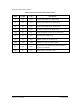


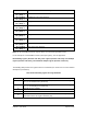
Table Of Contents
- List of Figures
- List of Tables
- 1. Introduction
- 1.1. Description
- 1.2. SPI Carrier Board
- 1.3. USB, CAN and SERIAL Carrier Board
- 1.4. Working Diagram
- 1.4.1. SPI Carrier Board
- 1.4.2. USB, CAN and SERIAL Board
- 2. Underlying Principles
- 3. Getting Started
- 3.1. Optional Power Supply
- 3.2. Optional SPI cable
- 3.3. Setup
- 3.4. Connecting to the LeddarVu Module
- 4. Measurements and Settings
- 4.1. Distance Measurement
- 4.2. Data Description
- 4.3. Acquisition Settings
- 4.3.1. General Settings
- 4.3.2. Enabling and Disabling Segments
- 4.4. Measurement Rate
- 4.5. CPU Load
- 5. Communication Interfaces
- 5.1. SPI Interface
- 5.1.1. SPI Basics
- 5.1.2. SPI Protocol
- 5.1.3. Memory Map
- Configuration Data
- Product Configuration
- Device Information and Constants
- LeddarVu Device Information and Constants
- General Status
- LeddarVu Status
- Detection List
- Transaction Configuration
- 5.1.4. SPI Operation
- 5.1.4.1. SPI Port Configuration
- 5.1.4.2. Sensor Hard Reset
- 5.1.4.3. Speed and timing
- 5.1.4.4. Access
- 5.1.4.5. Modification
- 5.2. I2C Interface
- 5.3. USB Interface
- 5.4. Serial Link Interface
- 5.5. CAN Bus Interface
- 6. Leddar™ Configurator
- 6.1. Introduction to Configurator Software
- 6.2. Connection Window
- 6.3. Leddar™ Configurator Main Window
- 6.3.1. Toolbar
- 6.3.2. Fit to Window
- 6.3.3. Force Equal Horizontal and Vertical Scales
- 6.3.4. Zoom in
- 6.3.5. Zoom out
- 6.3.6. Scale
- 6.3.7. Panning and Zooming
- 6.3.8. Changing the LeddarVu Module Origin
- 6.3.9. Changing the LeddarVu Module Orientation
- 6.4. Settings
- 6.4.1. Module Name
- 6.4.2. Acquisition Settings
- 6.4.3. Serial Port
- 6.4.4. CAN Port
- 6.5. Saving and Loading a Configuration
- 6.6. Configuring Detection Records
- 6.7. Using Detection Records
- 6.8. Data Logging
- 6.9. Firmware Update
- 6.10. Device State
- General
- Device Information
- Carrier
- 6.11. Preferences
- 6.12. Raw Detections
- 7. Specifications
- 7.1. General
- 7.2. Mechanical
- 7.3. Electrical
- 7.4. Optical
- 7.5. Performance
- 7.6. Regulatory Compliance and Safety
- 7.7. Dimensions
- 7.7.1. 98.5 Module
- 7.7.2. 47.5 Module
- 7.7.3. 16 Module
- 8. Technical Support
- Appendix A ̶ Example of a 0x04 function (read input register)
- Appendix B ̶ Example of a 0x41 Modbus Function
- Appendix C ̶ Example of a LeddarVu CAN Bus Detection Request

LeddarVu – User Guide Page 60 of 129
Address
Description
16 + (9*N) to
16 + (10*N) - 1
Distance of the fourth detection
16 + (10*N) to
16 + (11*N) - 1
Amplitude of the fourth detection
16 + (11*N) to
16 + (12*N) - 1
Flag of the fourth detection
16 + (12*N) to
16 + (13*N) - 1
Distance of fifth detection
16 + (13*N) to
16 + (14*N) - 1
Amplitude of fifth detection
16 + (14*N) to
16 + (15*N) - 1
Flag of the fifth detection
16 + (15*N) to
16 + (16*N) - 1
Distance of the sixth detection
16 + (16*N) to
16 + (17*N) - 1
Amplitude of the sixth detection
16 + (17*N) to
16 + (18*N) - 1
Flag of the sixth detection
NOTE: As per the Modbus protocol, register values are returned in big-endian format.
For an example of a 0x04 Modbus function (read input register), refer to Appendix A.
Read holding register (function code 0x3), write register (function code 0x6), write multiple
register (function code 0x10), and read/write multiple register (function code 0x17).
The following table presents the registers for these commands (see section 4.3 for a more detailed
description of parameters).
Table 28: Read holding register message definition
Address
Description
0
Exponent for the number of accumulations (that is, if the content of this register
is n, 2
n
accumulations are performed)
1
Exponent for the number of oversamplings (that is, if the content of this register
is n, 2
n
oversamplings are performed)
2
Number of base samples
3
Reserved
4
Detection threshold as a fixed-point value with a 6-bit fractional part (that is
threshold value is this register divided by 64).