
User Manual
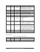
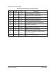


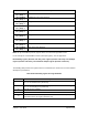
Table Of Contents
- List of Figures
- List of Tables
- 1. Introduction
- 1.1. Description
- 1.2. SPI Carrier Board
- 1.3. USB, CAN and SERIAL Carrier Board
- 1.4. Working Diagram
- 1.4.1. SPI Carrier Board
- 1.4.2. USB, CAN and SERIAL Board
- 2. Underlying Principles
- 3. Getting Started
- 3.1. Optional Power Supply
- 3.2. Optional SPI cable
- 3.3. Setup
- 3.4. Connecting to the LeddarVu Module
- 4. Measurements and Settings
- 4.1. Distance Measurement
- 4.2. Data Description
- 4.3. Acquisition Settings
- 4.3.1. General Settings
- 4.3.2. Enabling and Disabling Segments
- 4.4. Measurement Rate
- 4.5. CPU Load
- 5. Communication Interfaces
- 5.1. SPI Interface
- 5.1.1. SPI Basics
- 5.1.2. SPI Protocol
- 5.1.3. Memory Map
- Configuration Data
- Product Configuration
- Device Information and Constants
- LeddarVu Device Information and Constants
- General Status
- LeddarVu Status
- Detection List
- Transaction Configuration
- 5.1.4. SPI Operation
- 5.1.4.1. SPI Port Configuration
- 5.1.4.2. Sensor Hard Reset
- 5.1.4.3. Speed and timing
- 5.1.4.4. Access
- 5.1.4.5. Modification
- 5.2. I2C Interface
- 5.3. USB Interface
- 5.4. Serial Link Interface
- 5.5. CAN Bus Interface
- 6. Leddar™ Configurator
- 6.1. Introduction to Configurator Software
- 6.2. Connection Window
- 6.3. Leddar™ Configurator Main Window
- 6.3.1. Toolbar
- 6.3.2. Fit to Window
- 6.3.3. Force Equal Horizontal and Vertical Scales
- 6.3.4. Zoom in
- 6.3.5. Zoom out
- 6.3.6. Scale
- 6.3.7. Panning and Zooming
- 6.3.8. Changing the LeddarVu Module Origin
- 6.3.9. Changing the LeddarVu Module Orientation
- 6.4. Settings
- 6.4.1. Module Name
- 6.4.2. Acquisition Settings
- 6.4.3. Serial Port
- 6.4.4. CAN Port
- 6.5. Saving and Loading a Configuration
- 6.6. Configuring Detection Records
- 6.7. Using Detection Records
- 6.8. Data Logging
- 6.9. Firmware Update
- 6.10. Device State
- General
- Device Information
- Carrier
- 6.11. Preferences
- 6.12. Raw Detections
- 7. Specifications
- 7.1. General
- 7.2. Mechanical
- 7.3. Electrical
- 7.4. Optical
- 7.5. Performance
- 7.6. Regulatory Compliance and Safety
- 7.7. Dimensions
- 7.7.1. 98.5 Module
- 7.7.2. 47.5 Module
- 7.7.3. 16 Module
- 8. Technical Support
- Appendix A ̶ Example of a 0x04 function (read input register)
- Appendix B ̶ Example of a 0x41 Modbus Function
- Appendix C ̶ Example of a LeddarVu CAN Bus Detection Request

LeddarVu – User Guide Page 56 of 129
Transaction Configuration
Table 26: Transaction configuration bank
Offset
Length
Type
Description
0
1
uint8_t
Secure-transaction enabled flags:
1 = Enables the CRC calculation and validation on any
transaction. This flag is enabled by default.
0 = No CRC validation. The CRC field is still required in SPI
protocol but can be set to any value.
1
1
uint8_t
Transaction modes:
0 = Free run. The READY pin is asserted on each ready
detection frame. The host must be able to read data on time.
1 = Blocking read. On the READY pin assertion, host must
read all data from traces or detections bank (data transaction
control source configuration) to continue acquisition.
2 = Partial blocking read. On the READY pin assertion, host
can read all data from traces of the detection bank and the
acquisition is still running. Possible loss of detection frames
if the host reading data is very long.
2
2
uint16_t
CRC of the last transaction
4
2
uint16_t
Bit-field information of last transactions:
• All bits to 0: No transaction error
• Bit-0: Access right violation
• Bit-1: Invalid address
• Bit-2: Command not found
• Bit-3: Write disabled
• Bit-4: CRC failed
• Bit-5: Command execution error
• Bit-6: Invalid packet
6
1
uint8_t
Data transaction control source:
0 = On trace
1 = On detections
This register determines which data type will control the
READY pin and manage the transaction mode.