
User Manual
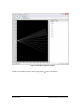
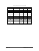
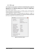


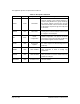
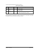


Table Of Contents
- List of Figures
- List of Tables
- 1. Introduction
- 1.1. Description
- 1.2. SPI Carrier Board
- 1.3. USB, CAN and SERIAL Carrier Board
- 1.4. Working Diagram
- 1.4.1. SPI Carrier Board
- 1.4.2. USB, CAN and SERIAL Board
- 2. Underlying Principles
- 3. Getting Started
- 3.1. Optional Power Supply
- 3.2. Optional SPI cable
- 3.3. Setup
- 3.4. Connecting to the LeddarVu Module
- 4. Measurements and Settings
- 4.1. Distance Measurement
- 4.2. Data Description
- 4.3. Acquisition Settings
- 4.3.1. General Settings
- 4.3.2. Enabling and Disabling Segments
- 4.4. Measurement Rate
- 4.5. CPU Load
- 5. Communication Interfaces
- 5.1. SPI Interface
- 5.1.1. SPI Basics
- 5.1.2. SPI Protocol
- 5.1.3. Memory Map
- Configuration Data
- Product Configuration
- Device Information and Constants
- LeddarVu Device Information and Constants
- General Status
- LeddarVu Status
- Detection List
- Transaction Configuration
- 5.1.4. SPI Operation
- 5.1.4.1. SPI Port Configuration
- 5.1.4.2. Sensor Hard Reset
- 5.1.4.3. Speed and timing
- 5.1.4.4. Access
- 5.1.4.5. Modification
- 5.2. I2C Interface
- 5.3. USB Interface
- 5.4. Serial Link Interface
- 5.5. CAN Bus Interface
- 6. Leddar™ Configurator
- 6.1. Introduction to Configurator Software
- 6.2. Connection Window
- 6.3. Leddar™ Configurator Main Window
- 6.3.1. Toolbar
- 6.3.2. Fit to Window
- 6.3.3. Force Equal Horizontal and Vertical Scales
- 6.3.4. Zoom in
- 6.3.5. Zoom out
- 6.3.6. Scale
- 6.3.7. Panning and Zooming
- 6.3.8. Changing the LeddarVu Module Origin
- 6.3.9. Changing the LeddarVu Module Orientation
- 6.4. Settings
- 6.4.1. Module Name
- 6.4.2. Acquisition Settings
- 6.4.3. Serial Port
- 6.4.4. CAN Port
- 6.5. Saving and Loading a Configuration
- 6.6. Configuring Detection Records
- 6.7. Using Detection Records
- 6.8. Data Logging
- 6.9. Firmware Update
- 6.10. Device State
- General
- Device Information
- Carrier
- 6.11. Preferences
- 6.12. Raw Detections
- 7. Specifications
- 7.1. General
- 7.2. Mechanical
- 7.3. Electrical
- 7.4. Optical
- 7.5. Performance
- 7.6. Regulatory Compliance and Safety
- 7.7. Dimensions
- 7.7.1. 98.5 Module
- 7.7.2. 47.5 Module
- 7.7.3. 16 Module
- 8. Technical Support
- Appendix A ̶ Example of a 0x04 function (read input register)
- Appendix B ̶ Example of a 0x41 Modbus Function
- Appendix C ̶ Example of a LeddarVu CAN Bus Detection Request

LeddarVu – User Guide Page 50 of 129
5.1.3. Memory Map
The memory map is divided in four memory banks. This section presents the description of the four
memory banks in a table format.
Table 17: Memory banks
Bank
Number
Start Base
Address
Bank Size
(KB)
Access
Description
0
0x00000000
1024
R/W
Configuration data
2
0x00200000
512
R/W
Configuration data
6
0x00400000
128
Read only
General device information and
constants
10
0x00480000
128
R/W
General Status
12
0x004C0000
128
R/W
LeddarVu Status
14
0x00500000
1024
Read only
Detection list
21
0x00FFFB00
1
R/W
Transaction configuration
Configuration Data
Table 18: Configuration data bank
Offset
Length
Type
Description
0
32
char
Module name as an ASCII string
32
1
uint8_t
Accumulation exponent: for example, 3 =
2
3
=8
33
1
uint8_t
Oversampling exponent: for example, 3 =
2
3
=8
34
1
uint8_t
Base point sample
35
4
uint32_t
Bit field of segment enabled
39
4
uint32_t
Acquisition rate of the reference pulse
43
4
float
Yaw angle of the module
47
4
float
Pitch angle of the module
51
4
float
Roll angle of the module
55
4
float
X-axis position of the module
59
4
float
Y-axis position of the module
63
4
float
Z-axis position of the module