
User Manual

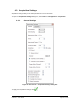


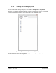
Table Of Contents
- List of Figures
- List of Tables
- 1. Introduction
- 1.1. Description
- 1.2. SPI Carrier Board
- 1.3. USB, CAN and SERIAL Carrier Board
- 1.4. Working Diagram
- 1.4.1. SPI Carrier Board
- 1.4.2. USB, CAN and SERIAL Board
- 2. Underlying Principles
- 3. Getting Started
- 3.1. Optional Power Supply
- 3.2. Optional SPI cable
- 3.3. Setup
- 3.4. Connecting to the LeddarVu Module
- 4. Measurements and Settings
- 4.1. Distance Measurement
- 4.2. Data Description
- 4.3. Acquisition Settings
- 4.3.1. General Settings
- 4.3.2. Enabling and Disabling Segments
- 4.4. Measurement Rate
- 4.5. CPU Load
- 5. Communication Interfaces
- 5.1. SPI Interface
- 5.1.1. SPI Basics
- 5.1.2. SPI Protocol
- 5.1.3. Memory Map
- Configuration Data
- Product Configuration
- Device Information and Constants
- LeddarVu Device Information and Constants
- General Status
- LeddarVu Status
- Detection List
- Transaction Configuration
- 5.1.4. SPI Operation
- 5.1.4.1. SPI Port Configuration
- 5.1.4.2. Sensor Hard Reset
- 5.1.4.3. Speed and timing
- 5.1.4.4. Access
- 5.1.4.5. Modification
- 5.2. I2C Interface
- 5.3. USB Interface
- 5.4. Serial Link Interface
- 5.5. CAN Bus Interface
- 6. Leddar™ Configurator
- 6.1. Introduction to Configurator Software
- 6.2. Connection Window
- 6.3. Leddar™ Configurator Main Window
- 6.3.1. Toolbar
- 6.3.2. Fit to Window
- 6.3.3. Force Equal Horizontal and Vertical Scales
- 6.3.4. Zoom in
- 6.3.5. Zoom out
- 6.3.6. Scale
- 6.3.7. Panning and Zooming
- 6.3.8. Changing the LeddarVu Module Origin
- 6.3.9. Changing the LeddarVu Module Orientation
- 6.4. Settings
- 6.4.1. Module Name
- 6.4.2. Acquisition Settings
- 6.4.3. Serial Port
- 6.4.4. CAN Port
- 6.5. Saving and Loading a Configuration
- 6.6. Configuring Detection Records
- 6.7. Using Detection Records
- 6.8. Data Logging
- 6.9. Firmware Update
- 6.10. Device State
- General
- Device Information
- Carrier
- 6.11. Preferences
- 6.12. Raw Detections
- 7. Specifications
- 7.1. General
- 7.2. Mechanical
- 7.3. Electrical
- 7.4. Optical
- 7.5. Performance
- 7.6. Regulatory Compliance and Safety
- 7.7. Dimensions
- 7.7.1. 98.5 Module
- 7.7.2. 47.5 Module
- 7.7.3. 16 Module
- 8. Technical Support
- Appendix A ̶ Example of a 0x04 function (read input register)
- Appendix B ̶ Example of a 0x41 Modbus Function
- Appendix C ̶ Example of a LeddarVu CAN Bus Detection Request

LeddarVu – User Guide Page 36 of 129
Threshold offset
The threshold offset is a value that modifies the detection amplitude threshold.
A default detection threshold table was determined to provide robust detection and minimize false
detections caused by noise in the input signal.
Figure 16 below presents the threshold table for a light source intensity of 16. This table is
effective when the threshold offset value is 0.
Figure 16: Detection threshold example
The multiple lines on each graph present the thresholds for numbers of accumulations of 1 (top
curve), 2, 4, 8, 16, 32, 64, 128, and 256 (bottom curve). Accumulations of 512 and 1024 are also
available, although not shown (provide the lowest thresholds).
The threshold offset parameter has the effect of offsetting each value in the threshold table by the
selected value. This provides a means of reducing the sensitivity (positive value) or increasing the
sensitivity (negative value) of the module. Increasing the value of the threshold offset allows
ignoring (will not result in a measurement) signals with amplitude higher than the default threshold.
Decreasing the value of the threshold offset allows measurements of amplitude signals lower than
the default threshold.
NOTE: The default setting (0) is selected to ensure a very low occurrence of false measurements.
False measurements are likely to occur when reducing the threshold offset (negative values).
These false measurements are very random in occurrence while true measurements will be
repeatable. For this reason, it may be useful in some applications to use a higher sensitivity and