
User Manual
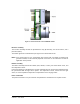
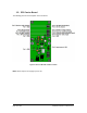
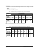

Table Of Contents
- List of Figures
- List of Tables
- 1. Introduction
- 1.1. Description
- 1.2. SPI Carrier Board
- 1.3. USB, CAN and SERIAL Carrier Board
- 1.4. Working Diagram
- 1.4.1. SPI Carrier Board
- 1.4.2. USB, CAN and SERIAL Board
- 2. Underlying Principles
- 3. Getting Started
- 3.1. Optional Power Supply
- 3.2. Optional SPI cable
- 3.3. Setup
- 3.4. Connecting to the LeddarVu Module
- 4. Measurements and Settings
- 4.1. Distance Measurement
- 4.2. Data Description
- 4.3. Acquisition Settings
- 4.3.1. General Settings
- 4.3.2. Enabling and Disabling Segments
- 4.4. Measurement Rate
- 4.5. CPU Load
- 5. Communication Interfaces
- 5.1. SPI Interface
- 5.1.1. SPI Basics
- 5.1.2. SPI Protocol
- 5.1.3. Memory Map
- Configuration Data
- Product Configuration
- Device Information and Constants
- LeddarVu Device Information and Constants
- General Status
- LeddarVu Status
- Detection List
- Transaction Configuration
- 5.1.4. SPI Operation
- 5.1.4.1. SPI Port Configuration
- 5.1.4.2. Sensor Hard Reset
- 5.1.4.3. Speed and timing
- 5.1.4.4. Access
- 5.1.4.5. Modification
- 5.2. I2C Interface
- 5.3. USB Interface
- 5.4. Serial Link Interface
- 5.5. CAN Bus Interface
- 6. Leddar™ Configurator
- 6.1. Introduction to Configurator Software
- 6.2. Connection Window
- 6.3. Leddar™ Configurator Main Window
- 6.3.1. Toolbar
- 6.3.2. Fit to Window
- 6.3.3. Force Equal Horizontal and Vertical Scales
- 6.3.4. Zoom in
- 6.3.5. Zoom out
- 6.3.6. Scale
- 6.3.7. Panning and Zooming
- 6.3.8. Changing the LeddarVu Module Origin
- 6.3.9. Changing the LeddarVu Module Orientation
- 6.4. Settings
- 6.4.1. Module Name
- 6.4.2. Acquisition Settings
- 6.4.3. Serial Port
- 6.4.4. CAN Port
- 6.5. Saving and Loading a Configuration
- 6.6. Configuring Detection Records
- 6.7. Using Detection Records
- 6.8. Data Logging
- 6.9. Firmware Update
- 6.10. Device State
- General
- Device Information
- Carrier
- 6.11. Preferences
- 6.12. Raw Detections
- 7. Specifications
- 7.1. General
- 7.2. Mechanical
- 7.3. Electrical
- 7.4. Optical
- 7.5. Performance
- 7.6. Regulatory Compliance and Safety
- 7.7. Dimensions
- 7.7.1. 98.5 Module
- 7.7.2. 47.5 Module
- 7.7.3. 16 Module
- 8. Technical Support
- Appendix A ̶ Example of a 0x04 function (read input register)
- Appendix B ̶ Example of a 0x41 Modbus Function
- Appendix C ̶ Example of a LeddarVu CAN Bus Detection Request

LeddarVu – User Guide Page 16 of 129
NOTES:
• DIP switch position 6 on ‘ON’ position enables a 121Ω termination resistor to RS-485 two-
wire configuration only (must be kept on ‘OFF’ position in any other configuration).
• DIP switch position 8 on ‘ON’ position enables a 121Ω termination resistor to CAN port.
Configurable serial link 1
Depending on the DIP switch positions, the configurable serial link pin functionalities differ
(refer to Table 3).
Table 3: Communication link configuration
Pin
position
Interface
RS-232
RS-485 two-wire
configuration
RS-422
RS-485 four-wire
configuration
1
GND
GND
GND
3
RTS
D -
Dout -
5
NC
NC
NC
7
RX
D -
Din +
9
TX
D +
Dout +
11
CTS
D -
Din -
NOTE: If a two-wire or four-wire differential port configuration is selected, in function of your network
configuration, you should put bias resistors on transmitter or receiver lines to maintain the
proper idle voltage and force the line to the idle condition.