
User's Manual
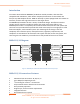
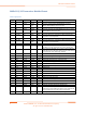
Table Of Contents
- Introduction
- MOD6212/13 Diagram
- MOD6212/13 transceiver Features
- 1
- 2
- 3
- 1
- 2
- 3
- MOD6212/13 Transceiver Module Dimensions
- 1
- 2
- 3
- 4
- MOD6212/13 Transceiver Module Pinout
- 1.
- 2.
- 3.
- 4.
- 5.
- MOD6212/13 Transceiver Module Connector
- MOD6212/13 Transceiver Module Functional description
- 1
- 2
- 3
- 4
- 5
- 6
- 7
- Modular approval for Lattice MOD6212/13 transmitter

Module Installation Guide
4 ©2017 SiBEAM, Inc., a Lattice Semiconductor company.
All rights reserved. CONFIDENTIAL
MOD6212/13 Transceiver Module Pinout
Table 1. Signal pinout
Pin Name Type Dir Group Description
1 3V3 Power Input Power 3.3V +/-5% power supply
2 SCL Digital
In/Out
O.D.
I
2
C
I
2
C Clock, Tunneling port. SB6210/SB6212 Connect to
Master; SB6211/SB6213 Connect to Slave
3 3V3 Power Input Power 3.3V +/-5% power supply
4
SDA
Digital
In/Out
O.D.
I
2
C
I
2
C Data, Tunneling port. SB6210/SB6212 Connect to Master;
SB6211/SB6213 Connect to Slave
5 3V3 Power Input Power 3.3V +/-5% power supply
6 SCL_DBG I2C Bi-Dir USB
I
2
C Data, Debug port. Connection to debug controller not
required for normal operation.
7 GND Power Power Ground
8 SDA_DBG I
2
C
In/Out
O.D.
Debug
I
2
C Data, Debug port. Connection to debug controller not
required for normal operation.
9 GND Power Power Ground
10 GPI Digital Input GPIO
General purpose input. Status of this input is reflected on
the GPO pin on the opposite side of an active wireless link.
11 WAKE_UP Digital Input Control
Force the link to W0 State. This is useful to bypass USB states,
when I2C tunnel or GPI signal needs to be used, while the link
is in low power states. Active High. Optional.
12
VBUS_SENSE
Digital
Input
USB
USB VBUS status input , 3V3
13 ATB_N Analog Output Debug Differential analog test bus - negative terminal
14
GND
Power
Power
Ground
15 ATB_P Analog Output Debug Differential analog test bus - positive terminal
16
SSRX-
Analog
Input
USB
USB Super speed Neg Input
17 RST Digital Input Config Reset Input, active HIGH
18
SSRX+
Analog
Input
USB
USB Super speed Pos Input
19 ID_IN Digital Input USB USB ID Input
20 GND Power Power Ground
21 ID_VAL Digital Input USB USB ID Valid Input
22 SSTX+ Analog Output USB USB Super speed Pos Output
23 ID_OUT Digital Output USB USB ID Output
24 SSTX- Analog Output USB USB Super speed Neg Output
25 VBUS_EN Digital Output USB USB VBUS status output, 3V3
26 GND Power Power Ground
27
LEDO
Digital
Output
Config
LED output
28 D+ Analog Bi-Dir USB USB High Speed/Full Speed/Low Speed Pos I/O
29
GPO/INT
Digital
Output
GPIO
General purpose output. When a wireless link is active, the
status of this output reflects the GPI pin on the opposite side
of the wireless link. Also used as I2C tunnel interupt
30 D- Analog Bi-Dir USB USB High Speed/Full Speed/Low Speed Neg I/O