
Technical Specs
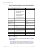
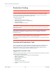
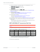
Table Of Contents
- Important Notice
- Safety and Hazards
- Limitation of Liability
- Contents
- List of Tables
- List of Figures
- 1: Introduction
- 2: Electrical Specifications
- 3: RF Specifications
- 4: Power
- 5: Software Interface
- 6: Mechanical and Environmental Specifica- tions
- 7: Regulatory Compliance and Industry Certifi- cations
- A: Antenna Specification
- B: Design Checklist
- C: Testing
- AT Command Entry Timing Requirement
- Acceptance Testing
- Certification Testing
- Production Testing
- Functional Production Test
- Quality Assurance Testing
- Suggested Testing Equipment
- Testing Assistance Provided by Lantronix, Inc.
- IOT/Operator Testing
- Extended AT Commands for Testing
- D: Packaging
- E: References
- F: Acronyms

Rev 5 May.21
64
41113694
B: Design Checklist
This chapter provides a summary of the design considerations mentioned throughout this
guide. This includes items relating to the power interface, RF integration, thermal
considerations, cabling issues, and so on.
Note: This is NOT an exhaustive list of design considerations. It is expected that you will employ
good design practices and engineering principles in your integration.
Table B-1:
Hardware Integration Design Considerations
Suggestion Section where discussed
Component
placement
If an ESD suppressor is not used on the host device, allow space on the SIM connector
for series resistors in layout. (Up to 100 Ω may be used depending on ESD testing
requirements).
SIM Implementation on
page 29
Minimize RF cable losses as these affect performance values listed in product
specification documents.
RF Connections on page 36
Antennas
Match the module/ antenna coax connections to 50 Ω—mismatched antenna
impedance and cable loss negatively affect RF performance.
RF Connections on page 36
If installing UMTS and CDMA modules in the same device, consider using separate
antennas for maximum performance.
Antenna and Cabling on
page 37
Power
Make sure the power supply can handle the maximum current specified for the module
type.
Power Consumption on
page 46
Limit the total impedance of VCC and GND connections to the SIM at the connector to
less than 1 Ω (including any trace impedance and lumped element components—
inductors, filters, etc.). All other lines must have a trace impedance less than 2 Ω.
SIM Implementation on
page 29
Decouple the VCC line close to the SIM socket. The longer the trace length
(impedance) from socket to module, the greater the capacitance requirement to meet
compliance tests.
SIM Implementation on
page 29
PCB signal routing
USB 2.0/3.0— Route these signals over 90 Ω differential lines on the PCB.
I2C port—If supported, route these signals away from noise-sensitive signals on the
PCB.
PCM port—If supported, route these signals away from noise-sensitive signals on the
PCB.
EMI/ ESD
Investigate sources of localized interference early in the design cycle.
Methods to Mitigate Decreased
Rx Performance on page 39
B