
Technical Specs
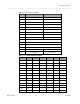
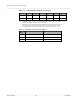
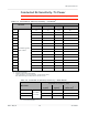
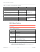
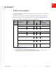
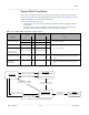

Table Of Contents
- Important Notice
- Safety and Hazards
- Limitation of Liability
- Contents
- List of Tables
- List of Figures
- 1: Introduction
- 2: Electrical Specifications
- 3: RF Specifications
- 4: Power
- 5: Software Interface
- 6: Mechanical and Environmental Specifica- tions
- 7: Regulatory Compliance and Industry Certifi- cations
- A: Antenna Specification
- B: Design Checklist
- C: Testing
- AT Command Entry Timing Requirement
- Acceptance Testing
- Certification Testing
- Production Testing
- Functional Production Test
- Quality Assurance Testing
- Suggested Testing Equipment
- Testing Assistance Provided by Lantronix, Inc.
- IOT/Operator Testing
- Extended AT Commands for Testing
- D: Packaging
- E: References
- F: Acronyms

Rev 5 May.21
50
41113694
t_USB_suspend
t_pwr_on_seq
t_USB_active
t_pwr_off_seq
t_pwr_on_seq
t_pwr_off _seq
t_pwr_on_seq
t_pwr_off
_seq
Disconnected Off
Power-off
Sequence
Active
Power-on
Sequence
Off Disconnected
Product
Technical
Specification
Power Interface
Power Ramp-up
On initial power up, inrush current depends on the power supply rise time— turn on time
>100 µs is required for < 3A inrush current.
The supply voltage must remain within specified tolerances while this is occurring.
Timing
Power On/Off Timing for the USB
Figure 4-2 describes the timing sequence for powering the module on and off.
Note: Before reaching the “Active” state, signals on the host port are considered to be undefined
and signal transitions may occur. This undefined state also applies when the module is in reset
mode, during a firmware update, or during the Power-off sequence. The host must consider these
undefined signal activities when designing the module interface.
Note: The host should not drive any signals to the module until >100 ms from the start of the
power-on sequence.
DEVICE STATE
VCC
High
Low
Full_Card_Power_Off#
USB_D+
(Double enumeration)
High
Low
High
Low
USB_D+
(Single enumeration)
High
Low
USB3.0
(Single enumeration)
High
Low
M.2 Host Signals
High
Low
Figure 4-2: Signal Timing (Full_Card_Power_Off#, and USB Enumeration)