
Technical Specs
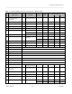
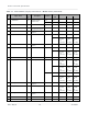
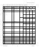
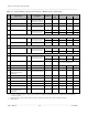
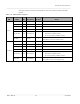
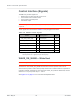
Table Of Contents
- Important Notice
- Safety and Hazards
- Limitation of Liability
- Contents
- List of Tables
- List of Figures
- 1: Introduction
- 2: Electrical Specifications
- 3: RF Specifications
- 4: Power
- 5: Software Interface
- 6: Mechanical and Environmental Specifica- tions
- 7: Regulatory Compliance and Industry Certifi- cations
- A: Antenna Specification
- B: Design Checklist
- C: Testing
- AT Command Entry Timing Requirement
- Acceptance Testing
- Certification Testing
- Production Testing
- Functional Production Test
- Quality Assurance Testing
- Suggested Testing Equipment
- Testing Assistance Provided by Lantronix, Inc.
- IOT/Operator Testing
- Extended AT Commands for Testing
- D: Packaging
- E: References
- F: Acronyms

Rev 5 May.21
24
41113694
Product
Technical
Specification
Table 2-1:
Host Interface (75-pin) Connections — Module View
a
(Continued)
Pin
Signal name
Pin
type
b
Description
Direction
c
Active
state
Voltage levels (V)
Min Typ Max
56 NC
Reserved—Host must
not repurpose this pin.
57 GND
V
Ground Input Power
- 0 -
58 NC
Reserved—Host must
not repurpose this pin.
59 ANTCTL0 (GPIO1)
Customer-defined
external switch control
for multiple antennas
Output High 1.35
-
1.80
Output Low
0 -
0.45
60 Reserved—Host must not repurpose this pin and should leave it not connected.
61 ANTCTL1 (GPIO2)
Customer-defined
external switch control
for multiple antennas
Output High 1.35
-
1.80
Output Low
0 -
0.45
TX_ON
Tx activity indicator Output High 1.35 1.80 1.90
62 Reserved—Host must not repurpose this pin and should leave it not connected.
63 ANTCTL2 (GPIO3)
Customer-defined
external switch control
for multiple antennas
Output High 1.35
-
1.80
Output Low
0 -
0.45
64 Reserved—Host must not repurpose this pin and should leave it not connected.
65 ANTCTL3 (GPIO4)
Customer-defined
external switch control
for multiple antennas
Output High 1.35
-
1.80
Output Low
0 -
0.45
66 SIM_DETECT
d
PU SIM indication Input
0 V—SIM not present
Open circuit—SIM present
67 RESET# PU Reset module Input Low
-
0.3
0.63
68 NC
Reserved
69
CONFIG_1
(GND in default module
configuration)
Reserved—Host must
not re-purpose this pin.
Output
-
0
70 VCC
V
Power source Input Power 3.135 3.7 4.4
71 GND
V
Ground Input Power
- 0 -
72 VCC
V
Power source Input Power 3.135 3.7 4.4
73 GND
V
Ground Input Power
- 0 -
74 VCC
V
Power source Input Power 3.135 3.7 4.4
75
CONFIG_2
(NC in default module
configuration)
V
Reserved Output
- -
-
a.
All values are preliminary and subject to change.
b.
I— Input; O—Digital output; OC—Open Collector output; PU—Digital input (internal pull up); PD— Digital input (internal pull down);
V—Power or ground
c.
Signal directions are from module’s point of view (e.g. ‘Output’ from module to host, ‘Input’ to module from host.)
d.
Required signal