
Data Sheet


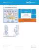
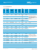
Table Of Contents
- 1 Overview and Key Features
- 1.2 Application Areas
- Features and Benefits
- 2 Specifications
- 3 Hardware Specifications
- 3.1 Block Diagram and Pin-out
- 3.2 Pin Definitions
- 3.3 Electrical Specifications
- 4 Functional Description
- 4.1 Power Management (includes brown-out and power on reset)
- 4.2 Clocks and Timers
- 4.3 RF
- 4.4 UART Interface
- 4.5 SPI Bus
- 4.6 I2C Interface
- 4.7 General Purpose I/O, ADC and PWM/FREQ
- 4.8 nRESET Pin
- 4.9 nAutoRUN Pin
- 4.10 RM1xx VSP Service and Modes
- 4.11 Two-Wire SWD Programming/Debug Interface
- 4.12 RM1xx on-board chip antenna characteristics
- 5 Hardware Integration Suggestions
- 6 Mechanical Details
- 7 Application Note for Surface Mount Modules
- 8 FCC and IC Regulatory Statements
- 9 CE Regulatory
- 10 EU Declarations of Conformity
- 11 Ordering Information
- 12 Bluetooth SIG Qualification

RM1xx LoRa/BLE Modules
Datasheet
https://connectivity.lairdtech.com/wireless-
modules/lorawan-solutions
9
© Copyright 2019 Laird. All Rights Reserved
Americas: +1-800-492-2320
Europe: +44-1628-858-940
Hong Kong: +852 2923 0610
3 HARDWARE SPECIFICATIONS
3.1 Block Diagram and Pin-out
Figure 1: Functional HW and SW block diagram for RM1xx series smartBASIC modules
Figure 2: RM186/RM191 module pin-out (top view)