
User's Manual
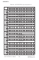


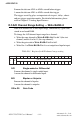

Table Of Contents
- Contents
- 1. Introduction
- 1.1 Features
- 1.2 Installation Guide
- 1.3 Accessories
- 2. Installation
- 2.1 Unpacking
- 2.2 Driver Installation
- 2.3 Hardware Installation
- 2.4 Device Setup & Configuration
- 2.5 Device Testing
- 3. Signal Connections
- 3.1 Overview
- 3.2 I/O Connector
- 3.3 Analog Input Connections
- 3.4 Analog Output Connections
- 3.5 Field Wiring Considerations
- 4. Software Overview
- 4.1 Programming Choices
- 4.2 DLL Driver Programming Roadmap
- 5. Principles of Operation
- 5.1 Analog Input Features
- 5.2 Analog Output Features
- 5.3 Digital I/O Features
- 5.4 Counter/Timer Features
- 6. Calibration
- 6.1 VR Assignment
- 6.2 A/D Calibration
- 6.3 D/A Calibration
- 6.4 Calibration Utility
- Appendix A. Specification
- Appendix B. Block Diagram
- Appendix C. Screw-terminal Board
- C. 1 Introduction
- C. 2 Features
- C. 3 Board Layout
- C.4 Pin Assignment
- C.5 Single-ended Connections
- C.6 Differential Connections
- Appendix D. Register Structure and Format
- D.1 Overview
- D.2 I/O Port Address Map
- D.3 A/D Single Value Acquisition - Write BASE+0
- D.4 Channel and A/D data - Read BASE + 0
- D.5 A/D Channel Range Setting - Write BASE+2
- D.6 MUX Control - Write BASE+4
- D.7 A/D Control/Status Register - Write/Read BASE+6
- D.8 Clear interrupt and FIFO - Write BASE+8
- D. 9 Interrupt and FIFO status - Read BASE+8
- D.10 D/A control/status register - Write/Read BASE+A
- D.11 D/A Channel 0/1 Data - Write BASE+C/E
- D.12 82C54 Counter Chip 0 - Write/Read BASE+10 to 16
- D.13 82C54 counter chip 1 - Write/Read BASE+18 to 1E
- D.14 Counter gate and clock control/status - Write/ Read BASE+20 to 26
- D.15 Digital I/O registers - Write/Read BASE+28
- D.16 Digital I/O configuration registers - Write/Read BASE+2A
- D.17 Calibration command registers - Write BASE+2C
- D.18 D/A Channel Data for Continuous Output Operation Mode - Write BASE+30
- Figures
- Figure 2-1: The Setup Screen of Advantech Automation Software
- Figure 2-2: Different options for Driver Setup
- Figure 2-3: The device name listed on the Device Manager
- Figure 2-4: The Advantech Device Installation utility program
- Figure 2-5: The I/O Device Installation dialog box
- Figure 2-6: The "Device(s) Found" dialog box
- Figure 2-7: The Device Setting dialog box
- Figure 2-8: The Device Name appearing on the list of devices box
- Figure 2-9: Analog Input tab on the Device Test dialog box
- Figure 2-10: Analog Input tab on the Device Test dialog box
- Figure 2-11: Analog Output tab on the Device Test dialog box
- Figure 2-12: Digital Input tab on the Device Test dialog box
- Figure 2-13: Digital Output tab on the Device Test dialog box
- Figure 2-14: Digital output tab on the Device Test dialog box
- Figure 3-1: I/O connector pin assignments for the PCI-1712/1712L
- Figure 3-2: Single-ended input channel connection
- Figure 3-3: Differential input channel connection - ground reference signal source
- Figure 3-4: Differential input channel connection - floating signal source
- Figure 3-5: Analog output connections
- Figure 5-1: Post-Trigger Acquisition Mode
- Figure 5-2: Delay-Trigger Acquisition Mode
- Figure 5-3: About-Trigger Acquisition Mode
- Figure 5-4: Pre-Trigger Acquisition Mode
- Figure 5-5: PCI-1712/1712L Sample Clock Source
- Figure 5-6: Frequency measurement
- Figure 6-1: PCI-1712/1712L VR1 & TP5
- Figure 6-2: Selecting the device you want to calibrate
- Figure 6-3: Warning message before start calibration
- Figure 6-4: Auto A/D Calibration Dialog Box
- Figure 6-5: A/D Calibration Procedure 1
- Figure 6-6: A/D Calibration Procedure 2
- Figure 6-7: A/D Calibration Procedure 3
- Figure 6-8: A/D Calibration is finished
- Figure 6-9: Range Selection in D/A Calibration
- Figure 6-10: Calibrating D/A Channel 0
- Figure 6-11: Calibrating D/A Channel 1
- Figure 6-12: D/A Calibration is finished
- Figure 6-13: Selecting Input Rage in Manual A/D Calibration panel
- Figure 6-14: Adjusting registers
- Figure 6-15: Selecting D/A Range and
- Figure 6-16: Selecting D/A Range and Choosing Output Voltage
- Figure 6-17: Adjusting registers
- Figure C-1: PCLD-8712 board layout
- Figure C-2: CN2 pin assignments for the PCLD-8712
- Tables
- Table 3-1: I/O Connector Signal Description (Part 1)
- Table 3-1: I/O Connector Signal Description (Part 2)
- Table 3-1: I/O Connector Signal Description (Part 3)
- Table 5-1: Gains and Analog Input Range
- Table 5-2: Analog Input Data Format
- Table 5-3: The corresponding Full Scale values for various Input Voltage Ranges
- Table 5-4: Analog Output Data Format
- Table 5-5: The corresponding Full Scale values for various Output Voltage Ranges
- Table D-1: PCI-1712/1712L register format (Part 1)
- Table D-1: PCI-1712/1712L register format (Part 2)
- Table D-1: PCI-1712/1712L register format (Part 3)
- Table D-2: Register for channel number and A/D data
- Table D-3: Register for A/D channel range setting
- Table D-4: Gain Codes for the PCI-1712/1712L
- Table D-5: Register for multiplexer control
- Table D-6: Register for A/D control/status
- Table D-7: Analog Input Acquisition Mode
- Table D-8: Register for clear interrupt and FIFO
- Table D-9: Register for interrupt and FIFO status
- Table D-10: Register for D/A control
- Table D-11: Analog output operation mode
- Table D-12: Register for D/A channel 0/1 data
- Table D-13: Register for 82C54 counter chip 0
- Table D-14: Register for 82C54 counter chip 1
- Table D-15: Register for counter gate and clock control/status
- Table D-16 : Table of Cn1 to Cn0 register
- Table D-17: Table of Gn1 to Gn0 register
- Table D-18: Table for CLK_SEL1 to CLK_SEL0 register
- Table D-19: Register for Digital I/O
- Table D-20: Register for digital I/O configuration
- Table D-21: Register for digital I/O configuration
- Table D-22: Register for calibration command
- Table D-23: Calibration command
- Table D-24: Register for D/A channel data
– 83 –
APPENDIX D
PCI-1712/1712L User’s Manual
Advantech Co., Ltd.
www.advantech.com
D.3 A/D Single Value Acquisition Write BASE+0
The A/D converter will convert one sample when you write to the
register Write BASE+0 with any value. User can check the A/D FIFO
status (A/D_F/E on register Read BASE+8) to make sure if the data is
ready to be received.
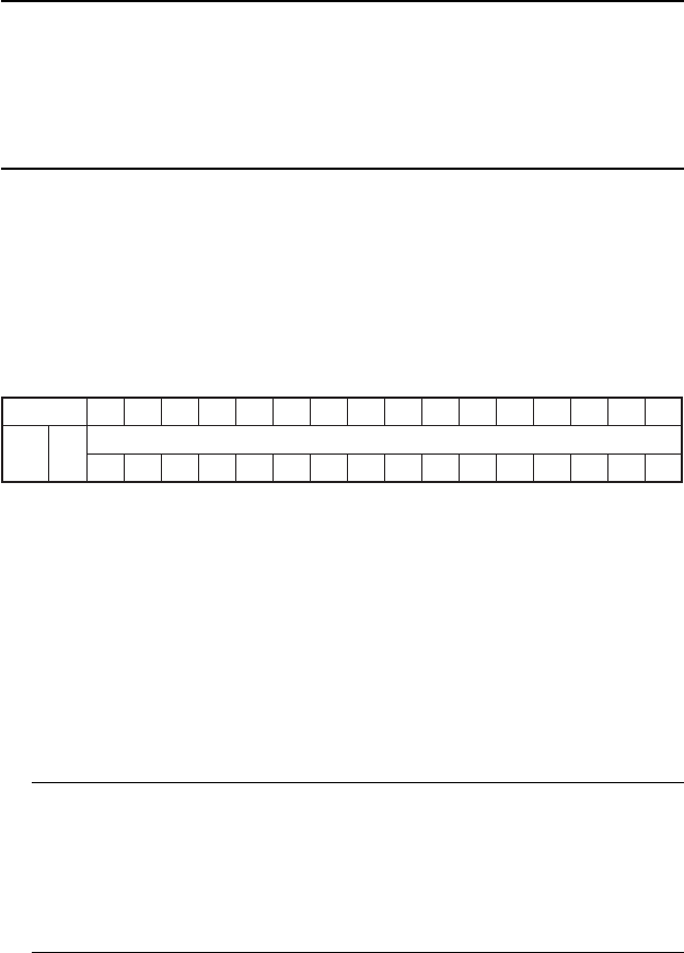
D.4 Channel and A/D data Read BASE + 0
These two bytes in Read BASE+0 hold the result of A/D conversion
data.
The 12 bits of data from the A/D conversion are stored in bit 0 to bit
11, bit 12 to 14 hold the A/D channel number and bit 15 holds the
trigger event flag.
Table D-2: Register for channel number and A/D data
AD11 TO AD0 Data of A/D Conversion
AD0 the least significant bit (LSB) of A/D data.
AD11 the most significant bit (MSB) of A/D data.
CH2 to CH0 A/D Channel Number
CH2 ~ CH0 hold the A/D channel number from which the data is
received.
CH2 MSB.
CH0 LSB.
Note:
✎ A/D channel number specifies the channel from which data is derived.
CH2 is the MSB and CH0 is the LSB. For channel scan, there should
have 4 channel codes, specifically from CH0 to CH3. Because we have
not enough address space, bit 15 is used for other purposes instead for
CH3, which is hence not available..
AF A/D trigger event flag
The trigger flag indicates whether a trigger event has happened during
A/D conversion process.
.ddAesaB 51 41 31 21 11 01 9 8 7 6 5 4 3 2 1 0
0 R
atadD/AdnalennahC
FA 2HC 1HC 0HC 11DA 01DA 9DA 8DA 7DA 6DA 5DA 4DA 3DA 2DA 1DA 0DA