
User's Manual
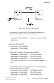


Table Of Contents
- Contents
- 1. Introduction
- 1.1 Features
- 1.2 Installation Guide
- 1.3 Accessories
- 2. Installation
- 2.1 Unpacking
- 2.2 Driver Installation
- 2.3 Hardware Installation
- 2.4 Device Setup & Configuration
- 2.5 Device Testing
- 3. Signal Connections
- 3.1 Overview
- 3.2 I/O Connector
- 3.3 Analog Input Connections
- 3.4 Analog Output Connections
- 3.5 Field Wiring Considerations
- 4. Software Overview
- 4.1 Programming Choices
- 4.2 DLL Driver Programming Roadmap
- 5. Principles of Operation
- 5.1 Analog Input Features
- 5.2 Analog Output Features
- 5.3 Digital I/O Features
- 5.4 Counter/Timer Features
- 6. Calibration
- 6.1 VR Assignment
- 6.2 A/D Calibration
- 6.3 D/A Calibration
- 6.4 Calibration Utility
- Appendix A. Specification
- Appendix B. Block Diagram
- Appendix C. Screw-terminal Board
- C. 1 Introduction
- C. 2 Features
- C. 3 Board Layout
- C.4 Pin Assignment
- C.5 Single-ended Connections
- C.6 Differential Connections
- Appendix D. Register Structure and Format
- D.1 Overview
- D.2 I/O Port Address Map
- D.3 A/D Single Value Acquisition - Write BASE+0
- D.4 Channel and A/D data - Read BASE + 0
- D.5 A/D Channel Range Setting - Write BASE+2
- D.6 MUX Control - Write BASE+4
- D.7 A/D Control/Status Register - Write/Read BASE+6
- D.8 Clear interrupt and FIFO - Write BASE+8
- D. 9 Interrupt and FIFO status - Read BASE+8
- D.10 D/A control/status register - Write/Read BASE+A
- D.11 D/A Channel 0/1 Data - Write BASE+C/E
- D.12 82C54 Counter Chip 0 - Write/Read BASE+10 to 16
- D.13 82C54 counter chip 1 - Write/Read BASE+18 to 1E
- D.14 Counter gate and clock control/status - Write/ Read BASE+20 to 26
- D.15 Digital I/O registers - Write/Read BASE+28
- D.16 Digital I/O configuration registers - Write/Read BASE+2A
- D.17 Calibration command registers - Write BASE+2C
- D.18 D/A Channel Data for Continuous Output Operation Mode - Write BASE+30
- Figures
- Figure 2-1: The Setup Screen of Advantech Automation Software
- Figure 2-2: Different options for Driver Setup
- Figure 2-3: The device name listed on the Device Manager
- Figure 2-4: The Advantech Device Installation utility program
- Figure 2-5: The I/O Device Installation dialog box
- Figure 2-6: The "Device(s) Found" dialog box
- Figure 2-7: The Device Setting dialog box
- Figure 2-8: The Device Name appearing on the list of devices box
- Figure 2-9: Analog Input tab on the Device Test dialog box
- Figure 2-10: Analog Input tab on the Device Test dialog box
- Figure 2-11: Analog Output tab on the Device Test dialog box
- Figure 2-12: Digital Input tab on the Device Test dialog box
- Figure 2-13: Digital Output tab on the Device Test dialog box
- Figure 2-14: Digital output tab on the Device Test dialog box
- Figure 3-1: I/O connector pin assignments for the PCI-1712/1712L
- Figure 3-2: Single-ended input channel connection
- Figure 3-3: Differential input channel connection - ground reference signal source
- Figure 3-4: Differential input channel connection - floating signal source
- Figure 3-5: Analog output connections
- Figure 5-1: Post-Trigger Acquisition Mode
- Figure 5-2: Delay-Trigger Acquisition Mode
- Figure 5-3: About-Trigger Acquisition Mode
- Figure 5-4: Pre-Trigger Acquisition Mode
- Figure 5-5: PCI-1712/1712L Sample Clock Source
- Figure 5-6: Frequency measurement
- Figure 6-1: PCI-1712/1712L VR1 & TP5
- Figure 6-2: Selecting the device you want to calibrate
- Figure 6-3: Warning message before start calibration
- Figure 6-4: Auto A/D Calibration Dialog Box
- Figure 6-5: A/D Calibration Procedure 1
- Figure 6-6: A/D Calibration Procedure 2
- Figure 6-7: A/D Calibration Procedure 3
- Figure 6-8: A/D Calibration is finished
- Figure 6-9: Range Selection in D/A Calibration
- Figure 6-10: Calibrating D/A Channel 0
- Figure 6-11: Calibrating D/A Channel 1
- Figure 6-12: D/A Calibration is finished
- Figure 6-13: Selecting Input Rage in Manual A/D Calibration panel
- Figure 6-14: Adjusting registers
- Figure 6-15: Selecting D/A Range and
- Figure 6-16: Selecting D/A Range and Choosing Output Voltage
- Figure 6-17: Adjusting registers
- Figure C-1: PCLD-8712 board layout
- Figure C-2: CN2 pin assignments for the PCLD-8712
- Tables
- Table 3-1: I/O Connector Signal Description (Part 1)
- Table 3-1: I/O Connector Signal Description (Part 2)
- Table 3-1: I/O Connector Signal Description (Part 3)
- Table 5-1: Gains and Analog Input Range
- Table 5-2: Analog Input Data Format
- Table 5-3: The corresponding Full Scale values for various Input Voltage Ranges
- Table 5-4: Analog Output Data Format
- Table 5-5: The corresponding Full Scale values for various Output Voltage Ranges
- Table D-1: PCI-1712/1712L register format (Part 1)
- Table D-1: PCI-1712/1712L register format (Part 2)
- Table D-1: PCI-1712/1712L register format (Part 3)
- Table D-2: Register for channel number and A/D data
- Table D-3: Register for A/D channel range setting
- Table D-4: Gain Codes for the PCI-1712/1712L
- Table D-5: Register for multiplexer control
- Table D-6: Register for A/D control/status
- Table D-7: Analog Input Acquisition Mode
- Table D-8: Register for clear interrupt and FIFO
- Table D-9: Register for interrupt and FIFO status
- Table D-10: Register for D/A control
- Table D-11: Analog output operation mode
- Table D-12: Register for D/A channel 0/1 data
- Table D-13: Register for 82C54 counter chip 0
- Table D-14: Register for 82C54 counter chip 1
- Table D-15: Register for counter gate and clock control/status
- Table D-16 : Table of Cn1 to Cn0 register
- Table D-17: Table of Gn1 to Gn0 register
- Table D-18: Table for CLK_SEL1 to CLK_SEL0 register
- Table D-19: Register for Digital I/O
- Table D-20: Register for digital I/O configuration
- Table D-21: Register for digital I/O configuration
- Table D-22: Register for calibration command
- Table D-23: Calibration command
- Table D-24: Register for D/A channel data

– 56 –
Chapter 6
PCI-1712/1712L User’s Manual
Advantech Co., Ltd.
www.advantech.com
6.2 A/D Calibration
Regular and proper calibration procedures ensure the maximum
possible accuracy. It is easy to complete the A/D calibration proce-
dure automatically (i.e. through software calibration) by executing the
A/D calibration program AutoCali. Therefore, it is not necessary to
adjust the hardware settings of the PCI-1712/1712L. However, the
following calibration steps are also provided for your reference in case
manual calibration is needed:
1. Adjust VR1 until the reference voltage on TP5 has reached
+5.0000 V.
2. Set PCI-1712 to calibration mode, which will configure AI2 to +5
V, and AI0 to 0 V. (Write “1” in AI0_CAL at the register address
BASE+6 bif7).
3. Adjust the PGA offset voltage. First, set the analog input voltage
range of AI0 to ±10V. Adjust the PGA offset register (BASE+2C),
and acquire a value from AI0 in single value acquisition mode.
Then switch the analog voltage range to ±1.25V to repeat the
operation in this step again to acquire a value from AI0. Repeat
this cycle several times. Meanwhile, adjust the PGA offset
voltage until the AI0’s values become the same for both the
analog input range ±10 V and ±1.25 V.
4. Adjust the gain value of the PGA. First, set the analog input
voltage range of AI2 between 0 and 5V. Adjust the gain register
(Base+2C), and then acquire the value for AI2 from single value
acquisition mode. Adjust the gain value of the PGA until the
subsequent AI2’s values converge within the Ox0ffe to
Ox0fff range.
5. Adjust the bipolar offset voltage. First, set the analog input
range within ±2.5 V. Adjust the bipolar offset register (Base+2C),
and then acquire the code from AI0 from single value acquisition
mode. Adjust the bipolar offset voltage until the AI0’s code
flickers around Ox0800.
6. Adjust unipolar offset voltage. First, set the analog input range
within 0 and 5 V. Adjust the unipolar offset register (Base+2C),
and then acquire the code for AI0 from single value acquisition