
Datasheet

VALUERAM0852-001.A00 Page 6
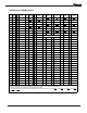
TECHNOLOGY
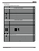
SPD Bus Interface Signals
5
SCL Serial Presence Detect (SPD) Clock Input 1
SDA SPD Data Input / Output 1
SA[2:0] SPD Address Inputs, also used to select the DIMM number in the AMB 3
Miscellaneous Signals
163
PLLTSTO PLL Clock Observability Output 1
VCCAPLL Analog VCC for the PLL. Tied with low pass filter to VCC. 1
VSSAPLL Analog VSS for the PLL. Tied to ground on the AMB die. Do not tie to ground on the DIMM. 1
TEST_pin# Leave floating on the DIMM 6
TESTLO_pin#
Tie to ground on the DIMM
2
5
BFUNC Tie to ground to set functionality as buffer on DIMM. 1
RESET
AMB reset signal 1
NC
No connect. Many NC are connected to VDD on the DIMM, to lower the impedance of the VDD power
islands.
129
RFU Reserved for Future Use 18
Power/Ground Signals
213
V
CC
AMB Core Power (1.5 Volt) 24
V
CCFBD
AMB Channel I/O Power (1.5 Volt) 8
V
DD
AMB DRAM I/O Power (1.8 Volt) 24
V
DDSPD
SPD Power (3.3 Volt) 1
V
SS
Ground 156
Total 655
1. System Clock Signals SCK and SCK switch at one half the DRAM CK/CK frequency.
2. TESTLO_AB20 and TESTLO_AC20 should be configured for debug purposes on prototype DIMMs: each pin should have a zero
ohm resistor pulldown to ground, and an unpopulated resistor pullup to VCC. These resistors can be replaced on production
DIMMs with a direct connection to ground.
Advanced Memory Buffer Pin Description: