
Datasheet
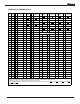
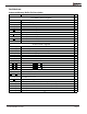

DIMM Connector Pin Description:
Pin Name Pin Description Count
SCK
System Clock Input, positive line
1
1
SCK
System Clock Input, negative line
1
1
PN[13:0] Primary Northbound Data, positive lines 14
PN
[13:0] Primary Northbound Data, negative lines 14
PS[9:0] Primary Southbound Data, positive lines 10
PS
[9:0] Primary Southbound Data, negative lines 10
SN[13:0] Secondary Northbound Data, positive lines 14
SN
[13:0] Secondary Northbound Data, negative lines 14
SS[9:0] Secondary Southbound Data, positive lines 10
SS
[9:0] Secondary Southbound Data, negative lines 10
SCL Serial Presence Detect (SPD) Clock Input 1
SDA SPD Data Input / Output 1
SA[2:0] SPD Address Inputs, also used to select the DIMM number in the AMB 3
VID[1:0]
Voltage ID: These pins must be unconnected for DDR2-based Fully Buffered DIMMs
VID[0] is V
DD
value: OPEN = 1.8 V, GND = 1.5 V; VID[1] is V
CC
value: OPEN = 1.5 V, GND = 1.2 V
2
RESET
AMB reset signal 1
RFU
Reserved for Future Use
2
16
V
CC
AMB Core Power and AMB Channel Interface Power (1.5 Volt) 8
V
DD
DRAM Power and AMB DRAM I/O Power (1.8 Volt) 24
V
TT
DRAM Address/Command/Clock Termination Power (V
DD
/2)
4
V
DDSPD
SPD Power 1
V
SS
Ground 80
DNU/M_Test
The DNU/M_Test pin provides an exter nal connection on R/Cs A-D for testing
the margin of Vref which is produced by a voltage divider on the module. It
is not intended to be used in normal system operation and must not be
connected (DNU) in a system. This test pin may have other features on future card designs
and if it does, will be included in this specification at that time.
1
1
Total 240
1. System Clock Signals SCK and SCK
switch at one half the DRAM CK/CK frequency
2. Eight pins reserved for forwarded clocks, eight pins reserved for future architecture flexibility
VALUERAM0852-001.A00 Page 3
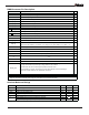
TECHNOLOGY
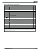
Absolute Maximum Ratings
095°C
AMB device operating temperature (Ambient)
0110°C
Symbol Parameter MIN MAX Units
V
IN, VOUT
Voltage on any pin relative to V
SS
-0.3 1.75 V
V
CC
Voltage on V
CC
pin relative to V
SS
-0.3 1.75 V
V
DD
Voltage V
DD
pin relative to Vss
-0.5 2.3 V
V
TT
Voltage on V
TT
pin relative to V
SS
-0.5 2.3 V
T
STG
Storage temperature
-55 100 °C
T
CASE
DDR2 SDRAM device operating temperature (Ambient)
Note: (1) Above 85°C DRAM case temperature the Auto-Refresh command interval has to be reduced to tREFI = 3.9 µs.
95
(1)