
User Manual


DS3234
Extremely Accurate SPI Bus RTC with
Integrated Crystal and SRAM
2 _____________________________________________________________________
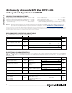
ABSOLUTE MAXIMUM RATINGS
RECOMMENDED OPERATING CONDITIONS
(T
A
= -40°C to +85°C, unless otherwise noted.) (Notes 2, 3)
Stresses beyond those listed under “Absolute Maximum Ratings” may cause permanent damage to the device. These are stress ratings only, and functional
operation of the device at these or any other conditions beyond those indicated in the operational sections of the specifications is not implied. Exposure to
absolute maximum rating conditions for extended periods may affect device reliability.
Voltage Range on Any Pin Relative to Ground......-0.3V to +6.0V
Junction-to-Ambient Thermal Resistance (θ
JA
) (Note 1) ...55°C/W
Junction-to-Case Thermal Resistance (θ
JC
) (Note 1) ........24°C/W
Operating Temperature Range
(noncondensing) .............................................-40°C to +85°C
Junction Temperature......................................................+125°C
Storage Temperature Range ...............................-40°C to +85°C
Lead Temperature (soldering, 10s) .................................+260°C
Soldering Temperature (reflow, 2 times max) ....................+260°C
(See the
Handling, PC Board Layout, and Assembly
section.)
PARAMETER SYMBOL CONDITIONS MIN TYP MAX UNITS
V
CC
2.0 3.3 5.5
Supply Voltage
V
BAT
2.0 3.0 3.8
V
Logic 1 Input CS, SCLK, DIN V
IH
0.7 x
V
CC
V
CC
+
0.3
V
2.0V V
CC
3.63V -0.3
+0.2 x
V
CC
Logic 0 Input CS, SCLK, DIN,
RST
V
IL
3.63V < V
CC
5.5V -0.3 +0.7
V
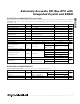
ELECTRICAL CHARACTERISTICS
(V
CC
= 2.0V to 5.5V, V
CC
= active supply (see Table 1), T
A
= -40°C to +85°C, unless otherwise noted.) (Typical values are at V
CC
=
3.3V, V
BAT
= 3.0V, and T
A
= +25°C, unless otherwise noted. TCXO operation guaranteed from 2.3V to 5.5V on V
CC
and 2.3V to 3.8V on
V
BAT
.) (Notes 2, 3)
PARAMETER SYMBOL CONDITIONS MIN TYP MAX UNITS
V
CC
= 3.63V 400
Active Supply Current I
CCA
SCLK = 4MHz, BSY = 0
(Notes 4, 5)
V
CC
= 5.5V 700
µA
V
CC
= 3.63V 120
Standby Supply Current I
CCS
CS = V
IH
, 32kHz output off,
SQW output off
(Note 5)
V
CC
= 5.5V 160
µA
V
CC
= 3.63V 500
Temperature Conversion Current I
CCSCONV
SPI bus inactive, 32kHz
output off, SQW output off
V
CC
= 5.5V 600
µA
Power-Fail Voltage V
PF
2.45 2.575 2.70 V
V
BAT
Leakage Current I
BATLKG
25 100 nA
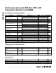
(V
CC
= 2.0V to 5.5V, T
A
= -40°C to +85°C, unless otherwise noted.) (Notes 2 and 3)
Logic 1 Output, 32kHz
I
OH
= -500µA
I
OH
= -250µA
I
OH
= -125µA
V
OH
V
CC
> 3.63V,
3.63V > V
CC
> 2.7V,
2.7V > (V
CC
or V
BAT
) > 2.0V
(BB32kHz = 1)
0.85 x V
CC
V
Note 1: Package thermal resistances were obtained using the method described in JEDEC specification JESD51-7, using a four-
layer board. For detailed information on package thermal considerations, refer to www.maxim-ic.com/thermal-tutorial
.