
User Manual


DS3234
Extremely Accurate SPI Bus RTC with
Integrated Crystal and SRAM
18 ____________________________________________________________________
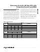
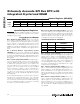
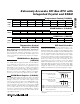
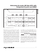
Address and data bytes are shifted MSB first into the
serial data input (DIN) and out of the serial data output
(DOUT). Any transfer requires the address of the byte
to specify a write or read, followed by one or more
bytes of data. Data is transferred out of the DOUT pin
for a read operation and into the DIN for a write opera-
tion (Figures 3 and 4).
The address byte is always the first byte entered after
CS is driven low. The most significant bit of this byte
determines if a read or write takes place. If the MSB is
0, one or more read cycles occur. If the MSB is 1, one
or more write cycles occur.
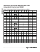
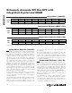
MODE
CS
SCLK DIN DOUT
Disable H
Input Disabled Input Disabled High Impedance
*CPOL = 1, SCLK Rising
Write L
CPOL = 0, SCLK Falling
Data Bit Latch High Impedance
CPOL = 1, SCLK Falling
Read L
CPOL = 0, SCLK Rising
X Next Data Bit Shift**
Read Invalid Location L Don’t Care
Don’t Care High Impedance
Table 3. SPI Pin Function
R/W
A6 A5 A4 A3 A2 A1 A0 D7 D6 D5 D4 D3 D2 D1 D0
CS
SCLK
DIN
DOUT
HIGH IMPEDANCE
Figure 3. SPI Single-Byte Write
A6 A5 A4 A3 A2 A1 A0
D7 D6 D5 D4 D3 D2 D1 D0
CS
SCLK
DIN
DOUT
HIGH IMPEDANCE
R/W
Figure 4. SPI Single-Byte Read
*
CPOL is the clock-polarity bit set in the control register of the host microprocessor.
**
DOUT remains at high impedance until 8 bits of data are ready to be shifted out during a read.