
User Manual


DS3234
Extremely Accurate SPI Bus RTC with
Integrated Crystal and SRAM
12 ____________________________________________________________________
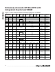
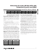
Figure 1. Address Map for DS3234 Timekeeping Registers and SRAM
Note: Unless otherwise specified, the registers’ state is not defined when power is first applied. Bits defined as 0 cannot be written
to 1 and will always read 0.
ADDRESS
READ/WRITE
MSB
BIT 7
BIT 6 BIT 5 BIT 4 BIT 3 BIT 2 BIT 1
LSB
BIT 0
FUNCTION RANGE
00h 80h 0 10 Seconds Seconds Seconds 00–59
01h 81h 0 10 Minutes Minutes Minutes 00–59
AM/PM
02h 82h 0 12/24
20 hr
10 hr Hour Hours
1-12 +AM /PM
00-23
03h 83h 0 0 0 0 0 Day Day 1-7
04h 84h 0 0 10 Date Date Date 01-31
05h 85h Century 0 0 10 Mo Month
Month/
Century
01-12 + Century
06h 86h 10 Year Year Year 00-99
07h 87h A1M1 10 Seconds Seconds
Alarm 1
Seconds
00-59
08h 88h A1M2 10 Minutes Minutes
Alarm 1
Minutes
00-59
AM/PM
09h 89h A1M3 12/24
20 hr
10 hr Hour
Alarm 1
Hours
1-12 +AM /PM
00-23
0Ah 8Ah A1M4 DY/DT
0
10 Date
Day
Date
Alarm 1 Day
Alarm 1 Date
1-7
01-31
0Bh 8Bh A2M2 10 Minutes Minutes
Alarm 2
Minutes
00-59
AM/PM
0Ch 8Ch A2M3 12/24
20 hr
10 hr Hour
Alarm 2
Hours
1-12 +AM /PM
00-23
0Dh 8Dh A2M4 DY/DT
0
10 Date
Day
Date
Alarm 2 Day
Alarm 2 Date
1-7
01-31
0Eh 8Eh EOSC BBSQW CONV RS2 RS1 INTCN A2IE A1IE Control —
0Fh 8Fh OSF BB32kHz CRATE1 CRATE0 EN32kHz BSY A2F A1F
Control/
Status
—
10h 90h SIGN DATA DATA DATA DATA DATA DATA DATA
Crystal Aging
Offset
—
11h 91h SIGN DATA DATA DATA DATA DATA DATA DATA Temp MSB Read Only
12h 92h DATA DATA 0 0 0 0 0 0 Temp LSB Read Only
13h 93h 0 0 0 0 0 0 0 BB_TD
Disable
Temp
Conversions
—
14h–17h 94h–97h — — — — — — — — Reserved —
18h 98h A7 A6 A5 A4 A3 A2 A1 A0
SRAM
Address
—
19h 99h D7 D6 D5 D4 D3 D2 D1 D0 SRAM Data —