
User Manual
D03Rev2.3
15
DMT proprietary & confidential: product information is subject to change without notice.
Domintech Co., Ltd. Tel: +886-2-2290-1288 Fax: +886-2-2290-1266 http://www.domintech.com.tw
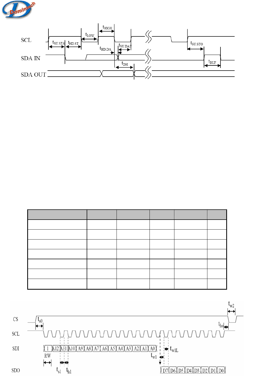
Figure 6: I2C Timing Diagram
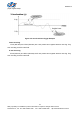
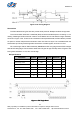
SPI Interface
The SPI interfaces using four-wire bus provide 22-bit protocols. Multiple read/write is supported.
The communication starts with a read/write (R/W) control bit with R/W equals 0 for writing or 1 for
reading. Following the R/W control bit comes a 13-bit address and an 8-bit data for single read/write,
as shown in Figure 7 & 8. To read 11-bit acceleration and temperature data, the SPI interface provides
an option to use the multiple read commands to read more than one byte. This is activated when the
serial enable pin CS stays active high after the read out of a data register, as shown in 9 & 10.
CS is active high. Data on SDI is latched by DMARD03 at SCL rising edge and the SDO changes
state at SCL falling edge. Communication starts when CS goes to high and stops when CS goes to low.
During these transitions on CS, SCL must be high.
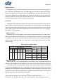
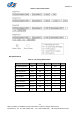
SPI Specifications
Parameter
ParameterParameter
Parameter
Symbol
SymbolSymbol
Symbol
Minimum
MinimumMinimum
Minimum
Typical
TypicalTypical
Typical
Maximum
MaximumMaximum
Maximum
Unit
UnitUnit
Unit
CS setup time
t
s0
300
—
—
ns
Data setup time
t
s1
150
—
—
ns
CS hold time
t
h0
150
—
—
ns
Data hold time
t
h1
150
—
—
ns
SCL pulse low width
t
w1L
160
—
—
ns
SCL pulse high width
t
w1H
160
—
—
ns
CS pulse low width
t
w2
1
—
—
µs
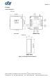
Figure 7
Figure 7Figure 7
Figure 7:
::
: SPI Single Read
SPI Single Read SPI Single Read
SPI Single Read