
User Manual


VS1003
4 CHARACTERISTICS & SPECIFICATIONS
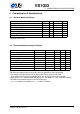
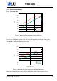
4.4 Power Consumption
Tested with an MPEG 1.0 Layer-3 128 kbit/s sample and generated sine. Output at full volume.
XTALI 12.288 MHz. Internal clock multiplier 3.0×. CVDD = 2.5 V, AVDD = 2.8 V.
Parameter Min Typ Max Unit
Power Supply Consumption AVDD, Reset 0.6 5.0 µA
Power Supply Consumption CVDD, Reset, +25
◦
C 3.7 40.0 µA
Power Supply Consumption CVDD, Reset, +85
◦
C 200.0 µA
Power Supply Consumption AVDD, sine test, 30Ω + GBUF 36.9 mA
Power Supply Consumption CVDD, sine test 12.4 mA
Power Supply Consumption AVDD, no load 7.0 mA
Power Supply Consumption AVDD, output load 30Ω 10.9 mA
Power Supply Consumption AVDD, 30Ω + GBUF 16.1 mA
Power Supply Consumption CVDD 17.5 mA
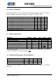
4.5 Digital Characteristics
Parameter Symbol Min Typ Max Unit
High-Level Input Voltage 0.7×IOVDD IOVDD+0.3
1
V
Low-Level Input Voltage -0.2 0.3×IOVDD V
High-Level Output Voltage at I
O
= -1.0 mA 0.7×IOVDD V
Low-Level Output Voltage at I
O
= 1.0 mA 0.3×IOVDD V
Input Leakage Current -1.0 1.0 µA
SPI Input Clock Frequency
2
CLKI
7
MHz
Rise time of all output pins, load = 50 pF 50 ns
1
Must not exceed 3.6V
2
Value for SCI reads. SCI and SDI writes allow
CLKI
4
.
4.6 Switching Characteristics - Boot Initialization
Parameter Symbol Min Max Unit
XRESET active time 2 XTALI
XRESET inactive to software ready 16600 50000
1
XTALI
Power on reset, rise time to CVDD 10 V/s
1
DREQ rises when initialization is complete. You should not send any data or commands
before that.
Version: 1.08, 2014-12-19 9