
User Manual


VS1003
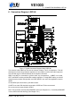
7 SPI BUSES
After the word has been shifted in and the last clock has been sent, XCS should be pulled high
to end the WRITE sequence.
After the last bit has been sent, DREQ is driven low for the duration of the register update,
marked “execution” in the figure. The time varies depending on the register and its contents
(see table in Chapter 8.6 for details). If the maximum time is longer than what it takes from
the microcontroller to feed the next SCI command or SDI byte, it is not allowed to finish a new
SCI/SDI operation before DREQ has risen up again.
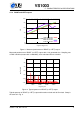
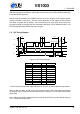
7.6 SPI Timing Diagram
XCS
SCK
SI
SO
0 1 1514 16
tXCSS
tXCSH
tWL tWH
tH
tSU
tV
tZ
tDIS
tXCS
30
31
Figure 12: SPI Timing Diagram.
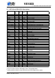
Symbol Min Max Unit
tXCSS 5 ns
tSU 0 ns
tH 2 CLKI cycles
tZ 0 ns
tWL 2 CLKI cycles
tWH 2 CLKI cycles
tV 2 (+ 25ns
1
) CLKI cycles
tXCSH 1 CLKI
tXCS 2 CLKI cycles
tDIS 10 ns
1
25ns is when pin loaded with 100pF capacitance. The time is shorter with lower capacitance.
Note: As tWL and tWH, as well as tH require at least 2 clock cycles, the maximum speed for
the SPI bus that can easily be used with asynchronous clocks is 1/7 of VS1003’s internal clock
speed CLKI.
Note: Although the timing is derived from the internal clock CLKI, the system always starts up
in 1.0× mode, thus CLKI=XTALI.
Version: 1.08, 2014-12-19 20