
User Manual


VS1003
7 SPI BUSES
7.5.2 SCI Read
0 1 2 3 4 5 6 7 8 9 10 11 12 13 30 3114 15 16 17
0 0 0 0 0 0 1 1 0 0 0 0
3 2 1 0
0 0 0 0 0 0 0 0 0 0 0 0 0 0 0 0
15 14 1 0
X
instruction (read) address
data out
XCS
SCK
SI
SO
don’t care don’t care
DREQ
execution
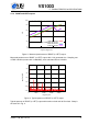
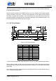
Figure 10: SCI Word Read
VS1003 registers are read from using the following sequence, as shown in Figure 10. First,
XCS line is pulled low to select the device. Then the READ opcode (0x3) is transmitted via
the SI line followed by an 8-bit word address. After the address has been read in, any further
data on SI is ignored by the chip. The 16-bit data corresponding to the received address will be
shifted out onto the SO line.
XCS should be driven high after data has been shifted out.
DREQ is driven low for a short while when in a read operation by the chip. This is a very short
time and doesn’t require special user attention.
7.5.3 SCI Write
0 1 2 3 4 5 6 7 8 9 10 11 12 13 30 3114 15 16 17
0 0 0 0 0 0 1 0 0 0 0
3 2 1 0
1 0
X
address
XCS
SCK
SI
15 14
data out
0 0 0 0 0 0 0 0 0 0 0 0 0 0 0 0SO
0 0 0 0
X
0
instruction (write)
DREQ
execution
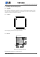
Figure 11: SCI Word Write
VS1003 registers are written from using the following sequence, as shown in Figure 11. First,
XCS line is pulled low to select the device. Then the WRITE opcode (0x2) is transmitted via the
SI line followed by an 8-bit word address.
Version: 1.08, 2014-12-19 19