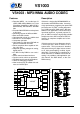
VS1003 VS1003 - MP3/WMA AUDIO CODEC Features Description • Decodes MPEG 1 & 2 audio layer III (CBR +VBR +ABR); WMA 4.0/4.1/7/8/9 all profiles (5-384kbit/s); WAV (PCM + IMA ADPCM); General MIDI / SP-MIDI files • Encodes IMA ADPCM from microphone or line input • Streaming support for MP3 and WAV • Bass and treble controls • Operates with a single 12..
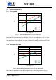
VS1003 CONTENTS Contents VS1003 1 Table of Contents 2 List of Figures 5 1 Licenses 6 2 Disclaimer 6 3 Definitions 6 4 Characteristics & Specifications 4.1 Absolute Maximum Ratings . . . . . . . . . 4.2 Recommended Operating Conditions . . . . 4.3 Analog Characteristics . . . . . . . . . . . . 4.4 Power Consumption . . . . . . . . . . . . . 4.5 Digital Characteristics . . . . . . . . . . . . . 4.6 Switching Characteristics - Boot Initialization 4.7 Typical characteristics . . . . . . . . . . .
VS1003 7.7.2 7.7.3 CONTENTS Two SDI Bytes . . . . . . . . . . . . . . . . . . . . . . . . . . . . . . . SCI Operation in Middle of Two SDI Bytes . . . . . . . . . . . . . . . 21 22 8 Functional Description 8.1 Main Features . . . . . . . . . . . . . . . . . . . . . . 8.2 Supported Audio Codecs . . . . . . . . . . . . . . . . 8.2.1 Supported MP3 (MPEG layer III) Formats 8.2.2 Supported WMA Formats . . . . . . . . . 8.2.3 Supported RIFF WAV Formats . . . . . . . 8.2.4 Supported MIDI Formats . . . . . . .
VS1003 10.4 SCI Registers . . . . . . . . . . . . . . . . . . . 10.5 Serial Data Registers . . . . . . . . . . . . . . . 10.6 DAC Registers . . . . . . . . . . . . . . . . . . . 10.7 GPIO Registers . . . . . . . . . . . . . . . . . . 10.8 Interrupt Registers . . . . . . . . . . . . . . . . 10.9 A/D Modulator Registers . . . . . . . . . . . . . 10.10 Watchdog v1.0 2002-08-26 . . . . . . . . . . . . 10.10.1 Registers . . . . . . . . . . . . . . . . 10.11 UART v1.0 2002-04-23 . . . . . . . . . . . . . . . 10.
VS1003 LIST OF FIGURES List of Figures 1 2 3 4 5 6 7 8 9 10 11 12 13 14 15 16 17 18 19 Measured ADC performance of the LINEIN pin. . . . . . . Measured ADC performance of the MIC pins (differential). Measured performance of RIGHT (or LEFT) output. . . . Typical spectrum of RIGHT (or LEFT) output. . . . . . . . Pin Configuration, LQFP-48. . . . . . . . . . . . . . . . . Pin Configuration, BGA-49. . . . . . . . . . . . . . . . . . Typical Connection Diagram Using LQFP-48. . . . . . . .
VS1003 1 3 DEFINITIONS Licenses MPEG Layer-3 audio decoding technology licensed from Fraunhofer IIS and Thomson. VS1003 contains WMA decoding technology from Microsoft. This product is protected by certain intellectual property rights of Microsoft and cannot be used or further distributed without a license from Microsoft. 2 Disclaimer All properties and figures are subject to change. 3 Definitions B Byte, 8 bits. b Bit. Ki “Kibi” = 210 = 1024 (IEC 60027-2). Mi “Mebi” = 220 = 1048576 (IEC 60027-2).
VS1003 4 4 4.1 Characteristics & Specifications Absolute Maximum Ratings Parameter Analog Positive Supply Digital Positive Supply I/O Positive Supply Current at Any Digital Output Voltage at Any Digital Input Operating Temperature Storage Temperature 1 CHARACTERISTICS & SPECIFICATIONS Symbol AVDD CVDD IOVDD Min -0.3 -0.3 -0.3 -0.3 -40 -65 Max 2.85 2.85 3.6 ±50 IOVDD+0.31 +85 +150 Unit V V V mA V ◦C ◦C Must not exceed 3.6 V 4.
VS1003 4 4.3 CHARACTERISTICS & SPECIFICATIONS Analog Characteristics Unless otherwise noted: AVDD=2.85V, CVDD=2.5V, IOVDD=-2.8V, TA=-25..+70◦ C, XTALI=12.288MHz, DAC tested with 1307.894 Hz full-scale output sinewave, measurement bandwidth 20..20000 Hz, analog output load: LEFT to GBUF 30Ω, RIGHT to GBUF 30Ω. Microphone test amplitude 50 mVpp, f=1 kHz, Line input test amplitude 2.2 Vpp, f=1 kHz.
VS1003 4 4.4 CHARACTERISTICS & SPECIFICATIONS Power Consumption Tested with an MPEG 1.0 Layer-3 128 kbit/s sample and generated sine. Output at full volume. XTALI 12.288 MHz. Internal clock multiplier 3.0×. CVDD = 2.5 V, AVDD = 2.8 V.
VS1003 4 4.7 4.7.1 CHARACTERISTICS & SPECIFICATIONS Typical characteristics Line input ADC 100 90 80 dB 70 60 50 40 SNR SNRa THD 30 20 0.001 0.01 0.1 input voltage (rms) 1 Figure 1: Measured ADC performance of the LINEIN pin. Measured ADC performance of the LINEIN pin. X-axis is rms amplitude of 1 kHz sine input. Curves are unweighted signal-to-noise ratio (blue), A-weighted signal-to-noise ratio (green), and unweighted signal-to-distortion ratio (red).
VS1003 4 4.7.3 CHARACTERISTICS & SPECIFICATIONS RIGHT and LEFT outputs 100 80 dB 60 40 SNR 30R LOAD SNR AWEIGHT 30R LOAD THD 30R LOAD THD NO LOAD 20 0 0.001 0.01 0.1 output voltage (rms) 1 Figure 3: Measured performance of RIGHT (or LEFT) output. Measured performance of RIGHT (or LEFT) output with 1 kHz generated sine. Sampling rate of DAC is 48 kHz (master clock 12.288 MHz), noise calculated from 0 to 20 kHz.
VS1003 5 5 PACKAGES AND PIN DESCRIPTIONS Packages and Pin Descriptions 5.1 Packages Both LPQFP-48 and BGA-49 are lead (Pb) free and also RoHS compliant packages. RoHS is a short name of Directive 2002/95/EC on the restriction of the use of certain hazardous substances in electrical and electronic equipment. 5.1.1 LQFP-48 48 1 Figure 5: Pin Configuration, LQFP-48. LQFP-48 package dimensions are at http://www.vlsi.fi/ . 5.1.2 BGA-49 A1 BALL PAD CORNER 1 2 4 3 5 6 7 A B 7.00 D 4.80 0.
VS1003 5 5.
VS1003 5 PACKAGES AND PIN DESCRIPTIONS Pin types: Type DI DO DIO DO3 AI Description Digital input, CMOS Input Pad Digital output, CMOS Input Pad Digital input/output Digital output, CMOS Tri-stated Output Pad Analog input Type AO AIO APWR DGND CPWR IOPWR Description Analog output Analog input/output Analog power supply pin Core or I/O ground pin Core power supply pin I/O power supply pin In BGA-49, no-connect balls are A7, B7, D4, E5, F1, G1. In LQFP-48, no-connect pins are 11, 12, 25, 35, 36.
VS1003 6 6 CONNECTION DIAGRAM, LQFP-48 Connection Diagram, LQFP-48 Figure 7: Typical Connection Diagram Using LQFP-48. The common buffer GBUF can be used for common voltage (1.24 V) for earphones. This will eliminate the need for large isolation capacitors on line outputs, and thus the audio output pins from VS1003 may be connected directly to the earphone connector. GBUF must NOT be connected to ground under any circumstances.
VS1003 7 7 SPI BUSES SPI Buses 7.1 General The SPI Bus - that was originally used in some Motorola devices - has been used for both VS1003’s Serial Data Interface SDI (Chapters 7.4 and 8.4) and Serial Control Interface SCI (Chapters 7.5 and 8.5). 7.2 SPI Bus Pin Descriptions 7.2.1 VS1002 Native Modes (New Mode) These modes are active on VS1003 when SM_SDINEW is set to 1 (default at startup).
VS1003 7.3 7 SPI BUSES Data Request Pin DREQ The DREQ pin/signal is used to signal if VS1003’s FIFO is capable of receiving data. If DREQ is high, VS1003 can take at least 32 bytes of SDI data or one SCI command. When these criteria are not met, DREQ is turned low, and the sender should stop transferring new data.
VS1003 7.4.3 7 SPI BUSES SDI in VS1001 Compatibility Mode BSYNC SDATA D7 D6 D5 D4 D3 D2 D1 D0 DCLK Figure 8: BSYNC Signal - one byte transfer. When VS1003 is running in VS1001 compatibility mode, a BSYNC signal must be generated to ensure correct bit-alignment of the input bitstream. The first DCLK sampling edge (rising or falling, depending on selected polarity), during which the BSYNC is high, marks the first bit of a byte (LSB, if LSB-first order is used, MSB, if MSB-first order is used).
VS1003 7.5.2 7 SPI BUSES SCI Read XCS 0 1 2 3 4 5 6 7 8 9 10 11 12 13 14 15 16 17 0 0 0 0 0 0 1 1 0 0 0 30 31 SCK 3 SI instruction (read) 2 1 0 don’t care 0 data out address 15 14 SO 0 0 0 0 0 0 0 0 0 0 0 0 0 don’t care 0 0 1 0 0 X execution DREQ Figure 10: SCI Word Read VS1003 registers are read from using the following sequence, as shown in Figure 10. First, XCS line is pulled low to select the device.
VS1003 7 SPI BUSES After the word has been shifted in and the last clock has been sent, XCS should be pulled high to end the WRITE sequence. After the last bit has been sent, DREQ is driven low for the duration of the register update, marked “execution” in the figure. The time varies depending on the register and its contents (see table in Chapter 8.6 for details).
VS1003 7.7 7.7.1 7 SPI BUSES SPI Examples with SM_SDINEW and SM_SDISHARED set Two SCI Writes SCI Write 1 SCI Write 2 XCS 0 1 2 3 30 31 1 0 32 33 61 62 63 2 1 0 SCK SI 0 0 0 X 0 0 X 0 DREQ up before finishing next SCI write DREQ Figure 13: Two SCI Operations. Figure 13 shows two consecutive SCI operations. Note that xCS must be raised to inactive state between the writes. Also DREQ must be respected as shown in the figure. 7.7.
VS1003 7.7.3 7 SPI BUSES SCI Operation in Middle of Two SDI Bytes SDI Byte SDI Byte SCI Operation XCS 0 7 1 8 9 39 40 41 7 6 46 47 1 0 SCK 7 6 5 1 0 0 SI 5 X 0 DREQ high before end of next transfer DREQ Figure 15: Two SDI Bytes Separated By an SCI Operation. Figure 15 shows how an SCI operation is embedded in between SDI operations. xCS edges are used to synchronize both SDI and SCI. Remember to respect DREQ as shown in the figure. Version: 1.
VS1003 8 8 FUNCTIONAL DESCRIPTION Functional Description 8.1 Main Features VS1003 is based on a proprietary digital signal processor, VS_DSP. It contains all the code and data memory needed for MP3, WMA and WAV PCM + ADPCM audio decoding, MIDI synthesizer, together with serial interfaces, a multirate stereo audio DAC and analog output amplifiers and filters. Also ADPCM audio encoding is supported using a microphone amplifier and A/D converter. A UART is provided for debugging purposes. 8.
VS1003 8.2.2 8 FUNCTIONAL DESCRIPTION Supported WMA Formats Windows Media Audio codec versions 2, 7, 8, and 9 are supported. All WMA profiles (L1, L2, and L3) are supported. Previously streams were separated into Classes 1, 2a, 2b, and 3. WMA 9 Professional and WMA 9 Lossless are not supported. The decoder has passed Microsoft’s conformance testing program. WMA 4.0 / 4.
VS1003 8.2.3 8 FUNCTIONAL DESCRIPTION Supported RIFF WAV Formats The most common RIFF WAV subformats are supported. Format 0x01 0x02 0x03 0x06 0x07 0x10 0x11 0x15 0x16 0x30 0x31 0x3b 0x3c 0x40 0x41 0x50 0x55 0x64 0x65 Name PCM ADPCM IEEE_FLOAT ALAW MULAW OKI_ADPCM IMA_ADPCM DIGISTD DIGIFIX DOLBY_AC2 GSM610 ROCKWELL_ADPCM ROCKWELL_DIGITALK G721_ADPCM G728_CELP MPEG MPEGLAYER3 G726_ADPCM G722_ADPCM Version: 1.
VS1003 8.2.4 8 FUNCTIONAL DESCRIPTION Supported MIDI Formats General MIDI and SP-MIDI format 0 files are played. Format 1 and 2 files must be converted to format 0 by the user. The maximum simultaneous polyphony is 40. Actual polyphony depends on the internal clock rate (which is user-selectable), the instruments used, and the possible postprocessing effects enabled, such as bass and treble enhancers. The polyphony restriction algorithm makes use of the SP-MIDI MIP table, if present. 36.86 MHz (3.
VS1003 8.3 SDI 8 FUNCTIONAL DESCRIPTION Data Flow of VS1003 Bitstream FIFO MP3/PlusV/ WAV/ADPCM/ WMA decode/ MIDI decode SM_ADPCM=0 AIADDR = 0 User Application AIADDR != 0 SB_AMPLITUDE=0 Bass enhancer SB_AMPLITUDE!=0 ST_AMPLITUDE=0 Treble enhancer ST_AMPLITUDE!=0 Volume control Audio FIFO SCI_VOL 2048 stereo samples L S.rate.conv. R and DAC Figure 16: Data Flow of VS1003.
VS1003 8.5 8 FUNCTIONAL DESCRIPTION Serial Control Interface (SCI) The serial control interface is compatible with the SPI bus specification. Data transfers are always 16 bits. VS1003 is controlled by writing and reading the registers of the interface. The main controls of the control interface are: • control of the operation mode, clock, and builtin effects • access to status information and header data • access to encoded digital data • uploading user programs 8.
VS1003 8.6.1 8 FUNCTIONAL DESCRIPTION SCI_MODE (RW) SCI_MODE is used to control the operation of VS1003 and defaults to 0x0800 (SM_SDINEW set).
VS1003 8 FUNCTIONAL DESCRIPTION SM_STREAM activates VS1003’s stream mode. In this mode, data should be sent with as even intervals as possible (and preferable with data blocks of less than 512 bytes), and VS1003 makes every attempt to keep its input buffer half full by changing its playback speed upto 5%. For best quality sound, the average speed error should be within 0.5%, the bitrate should not exceed 160 kbit/s and VBR should not be used. For details, see Application Notes for VS10XX.
VS1003 8.6.2 8 FUNCTIONAL DESCRIPTION SCI_STATUS (RW) SCI_STATUS contains information on the current status of VS1003 and lets the user shutdown the chip without audio glitches. Name SS_VER SS_APDOWN2 SS_APDOWN1 SS_AVOL Bits 6:4 3 2 1:0 Description Version Analog driver powerdown Analog internal powerdown Analog volume control SS_VER is 0 for VS1001, 1 for VS1011, 2 for VS1002 and 3 for VS1003. SS_APDOWN2 controls analog driver powerdown. Normally this bit is controlled by the system firmware.
VS1003 8.6.4 8 FUNCTIONAL DESCRIPTION SCI_CLOCKF (RW) The operation of SCI_CLOCKF is different in VS1003 than in VS1001, VS1011, and VS1002. Name SC_MULT SC_ADD SC_FREQ SCI_CLOCKF bits Bits Description 15:13 Clock multiplier 12:11 Allowed multiplier addition 10: 0 Clock frequency SC_MULT activates the built-in clock multiplier. This will multiply XTALI to create a higher CLKI.
VS1003 8.6.5 8 FUNCTIONAL DESCRIPTION SCI_DECODE_TIME (RW) When decoding correct data, current decoded time is shown in this register in full seconds. The user may change the value of this register. In that case the new value should be written twice. SCI_DECODE_TIME is reset at every software reset and also when WAV (PCM or IMA ADPCM), WMA, or MIDI decoding starts or ends. 8.6.
VS1003 8.6.9 8 FUNCTIONAL DESCRIPTION SCI_HDAT0 and SCI_HDAT1 (R) For WAV files, SCI_HDAT0 and SCI_HDAT1 read as 0x7761, and 0x7665, respectively. For WMA files, SCI_HDAT1 contains 0x574D and SCI_HDAT0 contains the data speed measured in bytes per second. To get the bit-rate of the file, multiply the value of SCI_HDAT0 by 8. for MIDI files, SCI_HDAT1 contains 0x4D54 and SCI_HDAT0 contains values according to the following table: HDAT0[15:8] 0 1..
VS1003 8 FUNCTIONAL DESCRIPTION When read, SCI_HDAT0 and SCI_HDAT1 contain header information that is extracted from MP3 stream currently being decoded. After reset both registers are cleared, indicating no data has been found yet.
VS1003 8.6.11 8 FUNCTIONAL DESCRIPTION SCI_VOL (RW) SCI_VOL is a volume control for the player hardware. For each channel, a value in the range of 0..254 may be defined to set its attenuation from the maximum volume level (in 0.5 dB steps). The left channel value is then multiplied by 256 and the values are added. Thus, maximum volume is 0 and total silence is 0xFEFE. Example: for a volume of -2.0 dB for the left channel and -3.5 dB for the right channel: (4*256) + 7 = 0x407.
VS1003 9 9.1 9 OPERATION Operation Clocking VS1003 operates on a single, nominally 12.288 MHz fundamental frequency master clock. This clock can be generated by external circuitry (connected to pin XTALI) or by the internal clock crystal interface (pins XTALI and XTALO). 9.2 Hardware Reset When the XRESET -signal is driven low, VS1003 is reset and all the control registers and internal states are set to the initial values. XRESET-signal is asynchronous to any external clock.
VS1003 9.4 9 OPERATION ADPCM Recording This chapter explains how to create RIFF/WAV file with IMA ADPCM format. This is a widely supported ADPCM format and many PC audio playback programs can play it. IMA ADPCM recording gives roughly a compression ratio of 4:1 compared to linear, 16-bit audio. This makes it possible to record 8 kHz audio at 32.44 kbit/s. 9.4.1 Activating ADPCM mode IMA ADPCM recording mode is activated by setting bits SM_RESET and SM_ADPCM in SCI_MODE.
VS1003 9 OPERATION Note: if SCI_HDAT1 ≥ 896, it may be better to wait for the buffer to overflow and clear before reading samples. That way you may avoid buffer aliasing. Each IMA ADPCM block is 128 words, i.e. 256 bytes. If you wish to interrupt reading data and possibly continue later, please stop at a 128-word boundary. This way whole blocks are skipped and the encoded stream stays valid. 9.4.
VS1003 9 OPERATION A way to see if you have written the file in the right way is to check bytes 2 and 3 (the first byte counts as byte 0) of each 256-byte block. Byte 3 should always be zero. 9.4.4 Playing ADPCM Data In order to play back your IMA ADPCM recordings, you have to have a file with a header as described in Chapter 9.4.3. If this is the case, all you need to do is to provide the ADPCM file through SDI as you would with any audio file. 9.4.
VS1003 void RecordAdpcm1003(void) { u_int16 w = 0, idx = 0; ... 9 OPERATION /* VS1003b/VS1033c */ /* Check and locate free space on disk */ SetMp3Vol(0x1414); WriteMp3SpiReg(SCI_BASS, /* Recording monitor volume */ 0); /* Bass/treble disabled */ WriteMp3SpiReg(SCI_CLOCKF, 0x4430); /* 2.0x 12.
VS1003 9.5 9 OPERATION SPI Boot If GPIO0 is set with a pull-up resistor to 1 at boot time, VS1003 tries to boot from external SPI memory. SPI boot redefines the following pins: Normal Mode GPIO0 GPIO1 DREQ GPIO2 SPI Boot Mode xCS CLK MOSI MISO The memory has to be an SPI Bus Serial EEPROM with 16-bit addresses (i.e. at least 1 KiB). The serial speed used by VS1003 is 245 kHz with the nominal 12.288 MHz clock. The first three bytes in the memory have to be 0x50, 0x26, 0x48.
VS1003 9.8 9 OPERATION SDI Tests There are several test modes in VS1003, which allow the user to perform memory tests, SCI bus tests, and several different sine wave tests. All tests are started in a similar way: VS1003 is hardware reset, SM_TESTS is set, and then a test command is sent to the SDI bus. Each test is started by sending a 4-byte special command sequence, followed by 4 zeros. The sequences are described below. 9.8.
VS1003 9.8.2 9 OPERATION Pin Test Pin test is activated with the 8-byte sequence 0x50 0xED 0x6E 0x54 0 0 0 0. This test is meant for chip production testing only. 9.8.3 Memory Test Memory test mode is initialized with the 8-byte sequence 0x4D 0xEA 0x6D 0x54 0 0 0 0. After this sequence, wait for 500000 clock cycles.
VS1003 10 10.1 10 VS1003 REGISTERS VS1003 Registers Who Needs to Read This Chapter User software is required when a user wishes to add some own functionality like DSP effects to VS1003. However, most users of VS1003 don’t need to worry about writing their own code, or about this chapter, including those who only download software plug-ins from VLSI Solution’s Web site. 10.2 The Processor Core VS_DSP is a 16/32-bit DSP processor core that also had extensive all-purpose processor features.
VS1003 Instruction (32−bit) 0000 0030 0500 X (16−bit) 10 VS1003 REGISTERS Y (16−bit) 0000 0030 System Vectors User Instruction RAM 0500 X DATA RAM Y DATA RAM User Space User Space Stack Stack 1800 1800 1880 1940 1880 1940 1C00 1C00 1E00 1E00 4000 4000 Instruction ROM X DATA ROM 8000 Y DATA ROM 8000 C000 C000 Hardware Register Space C100 C100 Figure 18: User’s Memory Map. 10.5 Serial Data Registers Reg 0xC011 0xC012 Type r w Reset 0 0 Version: 1.
VS1003 10.6 10 VS1003 REGISTERS DAC Registers Reg 0xC013 0xC014 0xC015 0xC016 Type rw rw rw rw Reset 0 0 0 0 DAC registers, prefix DAC_ Abbrev[bits] Description FCTLL DAC frequency control, 16 LSbs. FCTLH DAC frequency control 4MSbs, PLL control. LEFT DAC left channel PCM value. RIGHT DAC right channel PCM value. Every fourth clock cycle, an internal 26-bit counter is added to by (DAC_FCTLH & 15) × 65536 + DAC_FCTLL.
VS1003 10.8 10 VS1003 REGISTERS Interrupt Registers Reg 0xC01A 0xC01B 0xC01C 0xC01D Type rw w w rw Reset 0 0 0 0 Interrupt registers, prefix INT_ Abbrev[bits] Description ENABLE[7:0] Interrupt enable. GLOB_DIS[-] Write to add to interrupt counter. GLOB_ENA[-] Write to subtract from interript counter. COUNTER[4:0] Interrupt counter. INT_ENABLE controls the interrupts.
VS1003 10.9 10 VS1003 REGISTERS A/D Modulator Registers Reg 0xC01E 0xC01F Type rw rw Reset 0 0 Interrupt registers, prefix AD_ Abbrev[bits] Description DIV A/D Modulator divider. DATA A/D Modulator data. AD_DIV controls the AD converter’s sampling frequency. To gather one sample, 128 × n clock cycles are used (n is value of AD_DIV). The lowest usable value is 4, which gives a 48 kHz sample rate when CLKI is 24.576 MHz. When AD_DIV is 0, the A/D converter is turned off.
VS1003 10.10 10 VS1003 REGISTERS Watchdog v1.0 2002-08-26 The watchdog consist of a watchdog counter and some logic. After reset, the watchdog is inactive. The counter reload value can be set by writing to WDOG_CONFIG. The watchdog is activated by writing 0x4ea9 to register WDOG_RESET. Every time this is done, the watchdog counter is reset. Every 65536’th clock cycle the counter is decremented by one. If the counter underflows, it will activate vsdsp’s internal reset sequence.
VS1003 10.11 10 VS1003 REGISTERS UART v1.0 2002-04-23 RS232 UART implements a serial interface using rs232 standard. Start bit D0 D1 D2 D3 D4 D5 D6 Stop D7 bit Figure 19: RS232 Serial Interface Protocol When the line is idling, it stays in logic high state. When a byte is transmitted, the transmission begins with a start bit (logic zero) and continues with data bits (LSB first) and ends up with a stop bit (logic high). 10 bits are sent for each 8-bit byte frame. 10.11.
VS1003 10.11.3 10 VS1003 REGISTERS Data UARTx_DATA A read from UARTx_DATA returns the received byte in bits 7:0, bits 15:8 are returned as ’0’. If there is no more data to be read, the receiver data register full indicator will be cleared. A receive interrupt will be generated when a byte is moved from the receiver shift register to the receiver data register. A write to UARTx_DATA sets a byte for transmission. The data is taken from bits 7:0, other bits in the written value are ignored.
VS1003 10 VS1003 REGISTERS Example UART Speeds, fm = 26M Hz Comm. Speed [bps] UART_DIV_D1 UART_DIV_D2 4800 85 63 9600 42 63 14400 42 42 19200 51 26 28800 42 21 38400 25 26 57600 1 226 115200 0 226 10.11.6 Interrupts and Operation Transmitter operates as follows: After an 8-bit word is written to the transmit data register it will be transmitted instantly if the transmitter is not busy transmitting the previous byte. When the transmission begins a TX_INTR interrupt will be sent.
VS1003 10.12 10 VS1003 REGISTERS Timers v1.0 2002-04-23 There are two 32-bit timers that can be initialized and enabled independently of each other. If enabled, a timer initializes to its start value, written by a processor, and starts decrementing every clock cycle. When the value goes past zero, an interrupt is sent, and the timer initializes to the value in its start value register, and continues downcounting. A timer stays in that loop as long as it is enabled.
VS1003 10.12.3 VS1003 REGISTERS Configuration TIMER_ENABLE Name TIMER_EN_T1 TIMER_EN_T0 10.12.4 10 TIMER_ENABLE Bits Bits Description 1 Enable timer 1 0 Enable timer 0 Timer X Startvalue TIMER_Tx[L/H] The 32-bit start value TIMER_Tx[L/H] sets the initial counter value when the timer is reset. The fi timer interrupt frequency ft = c+1 where fi is the master clock obtained with the clock divider (see Chapter 10.12.2 and c is TIMER_Tx[L/H].
VS1003 10.13 10 VS1003 REGISTERS System Vector Tags The System Vector Tags are tags that may be replaced by the user to take control over several decoder functions. 10.13.1 AudioInt, 0x20 Normally contains the following VS_DSP assembly code: jmpi DAC_INT_ADDRESS,(i6)+1 The user may, at will, replace the first instruction with a jmpi command to gain control over the audio interrupt. 10.13.
VS1003 10 VS1003 REGISTERS The user may, at will, replace the instruction with a jmpi command to gain control over the AD Modulator interrupt. 10.13.5 TxInt, 0x24 Normally contains the following VS_DSP assembly code: jmpi EMPTY_INT_ADDRESS,(i6)+1 The user may, at will, replace the instruction with a jmpi command to gain control over the UART TX interrupt. 10.13.
VS1003 10.13.9 10 VS1003 REGISTERS UserCodec, 0x0 Normally contains the following VS_DSP assembly code: jr nop If the user wants to take control away from the standard decoder, the first instruction should be replaced with an appropriate j command to user’s own code. Unless the user is feeding MP3 or WMA data at the same time, the system activates the user program in less than 1 ms. After this, the user should steal interrupt vectors from the system, and insert user programs. 10.
VS1003 10.14.3 10 VS1003 REGISTERS DataBytes(), 0x6 VS_DSP C prototype: u_int16 DataBytes(void); If the user has taken over the normal operation of the system by switching the pointer in UserCodec to point to his own code, he may read data from the Data Interface through this and the following two functions. This function returns the number of data bytes that can be read. 10.14.4 GetDataByte(), 0x8 VS_DSP C prototype: u_int16 GetDataByte(void); Reads and returns one data byte from the Data Interface.
VS1003 11 11 LATEST DOCUMENT VERSION CHANGES Latest Document Version Changes This chapter describes the latest and most important changes to this document. Version 1.08, 2014-12-19 • Updated telephone number in Chapter 12, Contact Information. Version 1.07, 2014-03-11 • VS1003B-LK has been qualified for the same more relaxed CVDD limits as VS1003B-L and VS1003B-B. Because of this, the more strict CVDD limits for VS1003B-LK removed from Chapter 4.1, Absolute Maximum Ratings, and Chapter 4.
VS1003 12 12 CONTACT INFORMATION Contact Information VLSI Solution Oy Entrance G, 2nd floor Hermiankatu 8 FI-33720 Tampere FINLAND URL: http://www.vlsi.fi/ Phone: +358-50-462-3200 Commercial e-mail: sales@vlsi.fi For technical support or suggestions regarding this document, please participate at http://www.vsdsp-forum.com/ For confidential technical discussions, contact support@vlsi.fi Version: 1.