
User Manual


The ULN2001A is obsolete
a
nd is no longer supplied.
SLRS027G − DECEMBER 1976 − REVISED JUNE 2004
4
POST OFFICE BOX 655303 • DALLAS, TEXAS 75265
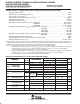
absolute maximum ratings at 25°C free-air temperature (unless otherwise noted)
†
Collector-emitter voltage 50 V. . . . . . . . . . . . . . . . . . . . . . . . . . . . . . . . . . . . . . . . . . . . . . . . . . . . . . . . . . . . . . . . . . . .
Clamp diode reverse voltage (see Note 1) 50 V. . . . . . . . . . . . . . . . . . . . . . . . . . . . . . . . . . . . . . . . . . . . . . . . . . . . .
Input voltage, V
I
(see Note 1) 30 V. . . . . . . . . . . . . . . . . . . . . . . . . . . . . . . . . . . . . . . . . . . . . . . . . . . . . . . . . . . . . . . .
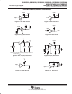
Peak collector current (see Figures 14 and 15) 500 mA. . . . . . . . . . . . . . . . . . . . . . . . . . . . . . . . . . . . . . . . . . . . .
Output clamp current, I
OK
500 mA. . . . . . . . . . . . . . . . . . . . . . . . . . . . . . . . . . . . . . . . . . . . . . . . . . . . . . . . . . . . . . . .
Total emitter-terminal current −2.5 A. . . . . . . . . . . . . . . . . . . . . . . . . . . . . . . . . . . . . . . . . . . . . . . . . . . . . . . . . . . . . .
Operating free-air temperature range, T
A
, ULN200xA −20°C to 70°C. . . . . . . . . . . . . . . . . . . . . . . . . . . . . . . . . .
ULQ200xA −40°C to 85°C. . . . . . . . . . . . . . . . . . . . . . . . . . . . . . . . .
ULQ200xAT −40°C to 105°C. . . . . . . . . . . . . . . . . . . . . . . . . . . . . . .
Package thermal impedance, θ
JA
(see Notes 2 and 3): D package 73°C/W. . . . . . . . . . . . . . . . . . . . . . . . . . . .
N package 67°C/W. . . . . . . . . . . . . . . . . . . . . . . . . . . .
NS package 64°C/W. . . . . . . . . . . . . . . . . . . . . . . . . . .
PW package 108°C/W. . . . . . . . . . . . . . . . . . . . . . . . .
Package thermal impedance, θ
JC
(see Notes 4 and 5): D package 36°C/W. . . . . . . . . . . . . . . . . . . . . . . . . . . .
N package 54°C/W. . . . . . . . . . . . . . . . . . . . . . . . . . . .
Operating virtual junction temperature, T
J
150°C. . . . . . . . . . . . . . . . . . . . . . . . . . . . . . . . . . . . . . . . . . . . . . . . . . .
Lead temperature 1,6 mm (1/16 inch) from case for 10 seconds 260°C. . . . . . . . . . . . . . . . . . . . . . . . . . . . . . .
Storage temperature range, T
stg
−65°C to 150°C. . . . . . . . . . . . . . . . . . . . . . . . . . . . . . . . . . . . . . . . . . . . . . . . . . .
†
Stresses beyond those listed under “absolute maximum ratings” may cause permanent damage to the device. These are stress ratings only, and
functional operation of the device at these or any other conditions beyond those indicated under “recommended operating conditions” is not
implied. Exposure to absolute-maximum-rated conditions for extended periods may affect device reliability.
NOTES: 1. All voltage values are with respect to the emitter/substrate terminal E, unless otherwise noted.
2. Maximum power dissipation is a function of T
J
(max), θ
JA
, and T
A
. The maximum allowable power dissipation at any allowable
ambient temperature is P
D
= (T
J
(max) − T
A
)/θ
JA
. Operating at the absolute maximum T
J
of 150°C can affect reliability.
3. The package thermal impedance is calculated in accordance with JESD 51-7.
4. Maximum power dissipation is a function of T
J
(max), θ
JC
, and T
C
. The maximum allowable power dissipation at any allowable case
temperature is P
D
= (T
J
(max) − T
C
)/θ
JC
. Operating at the absolute maximum T
J
of 150°C can affect reliability.
5. The package thermal impedance is calculated in accordance with MIL-STD-883.
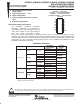
electrical characteristics, T
A
= 25°C (unless otherwise noted)
PARAMETER
TEST
TEST CONDITIONS
ULN2001A ULN2002A
UNIT
PARAMETER
TEST
FIGURE
TEST CONDITIONS
MIN TYP MAX MIN TYP MAX
UNIT
V
I(on)
On-state input voltage 6 V
CE
= 2 V, I
C
= 300 mA 13 V
Collector-emitter
I
I
= 250 µA, I
C
= 100 mA 0.9 1.1 0.9 1.1
V
CE(sat)
Collector-emitter
saturation voltage
5
I
I
= 350 µA, I
C
= 200 mA 1 1.3 1 1.3
V
V
CE(sat)
saturation voltage
5
I
I
= 500 µA, I
C
= 350 mA 1.2 1.6 1.2 1.6
V
V
F
Clamp forward voltage 8 I
F
= 350 mA 1.7 2 1.7 2 V
1 V
CE
= 50 V, I
I
= 0 50 50
I
CEX
Collector cutoff current
2
V
CE
= 50 V,
I
I
= 0 100 100
µA
I
CEX
Collector cutoff current
2
V
CE
= 50 V,
T
A
= 70°C
V
I
= 6 V 500
µA
I
I(off)
Off-state input current
3
V
CE
= 50 V,
I
C
= 500 µA
,
50
65
50
65
A
I
I(off)
Off-state input current 3
V
CE
= 50 V,
T
A
= 70°C
I
C
= 500 µA,
50 65 50 65 µA
I
I
Input current 4 V
I
= 17 V 0.82 1.25 mA
I
R
Clamp reverse current
7
V
R
= 50 V, T
A
= 70°C 100 100
A
I
R
Clamp reverse current 7
V
R
= 50 V 50 50
µA
h
FE
Static forward-current
transfer ratio
5 V
CE
= 2 V, I
C
= 350 mA 1000
C
i
Input capacitance V
I
= 0, f = 1 MHz 15 25 15 25 pF