
User Manual
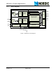

Revision 1.0 Page 7 of 78
nRF24L01+ Product Specification
1 Introduction
The nRF24L01+ is a single chip 2.4GHz transceiver with an embedded baseband protocol engine
(Enhanced ShockBurst™), suitable for ultra low power wireless applications. The nRF24L01+ is designed
for operation in the world wide ISM frequency band at 2.400 - 2.4835GHz.
To design a radio system with the nRF24L01+, you simply need an MCU (microcontroller) and a few exter-
nal passive components.
You can operate and configure the nRF24L01+ through a Serial Peripheral Interface (SPI). The register
map, which is accessible through the SPI, contains all configuration registers in the nRF24L01+ and is
accessible in all operation modes of the chip.
The embedded baseband protocol engine (Enhanced ShockBurst™) is based on packet communication
and supports various modes from manual operation to advanced autonomous protocol operation. Internal
FIFOs ensure a smooth data flow between the radio front end and the system’s MCU. Enhanced Shock-
Burst™ reduces system cost by handling all the high speed link layer operations.
The radio front end uses GFSK modulation. It has user configurable parameters like frequency channel,
output power and air data rate. nRF24L01+ supports an air data rate of 250 kbps, 1 Mbps and 2Mbps. The
high air data rate combined with two power saving modes make the nRF24L01+ very suitable for ultra low
power designs.
nRF24L01+ is drop-in compatible with nRF24L01 and on-air compatible with nRF2401A, nRF2402,
nRF24E1 and nRF24E2. Intermodulation and wideband blocking values in nRF24L01+ are much
improved in comparison to the nRF24L01 and the addition of internal filtering to nRF24L01+ has improved
the margins for meeting RF regulatory standards.
Internal voltage regulators ensure a high Power Supply Rejection Ratio (PSRR) and a wide power supply
range.