
User Manual


Revision 1.0 Page 67 of 78
nRF24L01+ Product Specification
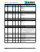
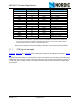
Table 29. Recommended components (BOM) in nRF24L01+ with antenna matching network
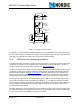
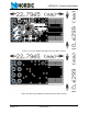
11.1 PCB layout examples
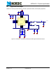
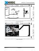
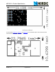
Figure 33., Figure 34. and Figure 35. show a PCB layout example for the application schematic in Figure
32..
A double-sided FR-4 board of 1.6mm thickness is used. This PCB has a ground plane on the bottom layer.
Additionally, there are ground areas on the component side of the board to ensure sufficient grounding of
critical components. A large number of via holes connect the top layer ground areas to the bottom layer
ground plane.
Part Designator Footprint Description
22pF
a
C1 0402 NPO, +/- 2%
22pF
a
C2 0402 NPO, +/- 2%
2.2nF C3 0402 X7R, +/- 10%
4.7pF C4 0402 NPO, +/- 0.25pF
1.5pF C5 0402 NPO, +/- 0.1pF
1,0pF C6 0402 NPO, +/- 0.1pF
33nF C7 0402 X7R, +/- 10%
1nF C8 0402 X7R, +/- 10%
10nF C9 0402 X7R, +/- 10%
8,2nH L1 0402 chip inductor +/- 5%
2.7nH L2 0402 chip inductor +/- 5%
3,9nH L3 0402 chip inductor +/- 5%
Not mounted
b
R1 0402
22k
Ω R2 0402 +/-1%
nRF24L01+ U1 QFN20 4x4
16MHz X1 +/-60ppm, C
L
=12pF
a. C1 and C2 must have values that match the crystals load capacitance, C
L.
b. The nRF24L01+ and nRF24L01 application example and BOM are the same with the exception of
R1. R1 can be mounted for backward compatibility with nRF24L01. The use of a 1Mohm resistor
externally does not have any impact on crystal performance.