
User Manual

Revision 1.0 Page 57 of 78
nRF24L01+ Product Specification
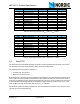
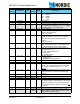
9 Register Map
You can configure and control the radio by accessing the register map through the SPI.
9.1 Register map table
All undefined bits in the table below are redundant. They are read out as '0'.
Note: Addresses 18 to 1B are reserved for test purposes, altering them makes the chip malfunction.
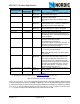
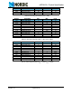
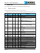
Address
(Hex)
Mnemonic Bit
Reset
Value
Type Description
00 CONFIG Configuration Register
Reserved 7 0 R/W Only '0' allowed
MASK_RX_DR 6 0 R/W Mask interrupt caused by RX_DR
1: Interrupt not reflected on the IRQ pin
0: Reflect RX_DR as active low interrupt on the
IRQ pin
MASK_TX_DS 5 0 R/W Mask interrupt caused by TX_DS
1: Interrupt not reflected on the IRQ pin
0: Reflect
TX_DS as active low interrupt on the IRQ
pin
MASK_MAX_RT 4 0 R/W Mask interrupt caused by MAX_RT
1: Interrupt not reflected on the IRQ pin
0: Reflect
MAX_RT as active low interrupt on the
IRQ pin
EN_CRC 3 1 R/W Enable CRC. Forced high if one of the bits in the
EN_AA is high
CRCO 2 0 R/W CRC encoding scheme
'0' - 1 byte
'1' – 2 bytes
PWR_UP 1 0 R/W 1: POWER UP, 0:POWER DOWN
PRIM_RX 00R/WRX/TX control
1: PRX, 0: PTX
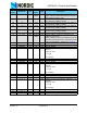
01 EN_AA
Enhanced
ShockBurst™
Enable ‘Auto Acknowledgment’ Function Disable
this functionality to be compatible with nRF2401,
see page 75
Reserved 7:6 00 R/W Only '00' allowed
ENAA_P5 5 1 R/W Enable auto acknowledgement data pipe 5
ENAA_P4 4 1 R/W Enable auto acknowledgement data pipe 4
ENAA_P3 3 1 R/W Enable auto acknowledgement data pipe 3
ENAA_P2 2 1 R/W Enable auto acknowledgement data pipe 2
ENAA_P1 1 1 R/W Enable auto acknowledgement data pipe 1
ENAA_P0 0 1 R/W Enable auto acknowledgement data pipe 0
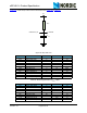
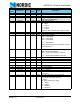
02 EN_RXADDR Enabled RX Addresses
Reserved 7:6 00 R/W Only '00' allowed
ERX_P5 5 0 R/W Enable data pipe 5.
ERX_P4 4 0 R/W Enable data pipe 4.
ERX_P3 3 0 R/W Enable data pipe 3.
ERX_P2 2 0 R/W Enable data pipe 2.