
User Manual

Revision 1.0 Page 11 of 78
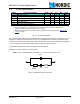
nRF24L01+ Product Specification
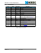
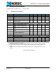
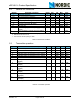
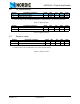
2.2 Pin functions
Table 1. nRF24L01+ pin function
Pin Name Pin function Description
1 CE Digital Input Chip Enable Activates RX or TX mode
2 CSN Digital Input SPI Chip Select
3 SCK Digital Input SPI Clock
4 MOSI Digital Input SPI Slave Data Input
5 MISO Digital Output SPI Slave Data Output, with tri-state option
6 IRQ Digital Output Maskable interrupt pin. Active low
7 VDD Power Power Supply (+1.9V - +3.6V DC)
8 VSS Power Ground (0V)
9 XC2 Analog Output Crystal Pin 2
10 XC1 Analog Input Crystal Pin 1
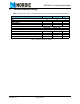
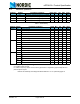
11 VDD_PA Power Output Power Supply Output (+1.8V) for the internal
nRF24L01+ Power Amplifier. Must be connected
to ANT1 and ANT2 as shown in Figure 32.
12 ANT1 RF Antenna interface 1
13 ANT2 RF Antenna interface 2
14 VSS Power Ground (0V)
15 VDD Power Power Supply (+1.9V - +3.6V DC)
16 IREF Analog Input Reference current. Connect a 22kΩ resistor to
ground. See Figure 32.
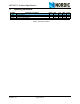
17 VSS Power Ground (0V)
18 VDD Power Power Supply (+1.9V - +3.6V DC)
19 DVDD Power Output Internal digital supply output for de-coupling pur-
poses. See Figure 32.
20 VSS Power Ground (0V)