nRF24L01+ Single Chip 2.4GHz Transceiver Product Specification v1.0 Key Features • • • • • • • • • • • • • • • • • • • Worldwide 2.4GHz ISM band operation 250kbps, 1Mbps and 2Mbps on air data rates Ultra low power operation 11.3mA TX at 0dBm output power 13.5mA RX at 2Mbps air data rate 900nA in power down 26µA in standby-I On chip voltage regulator 1.9 to 3.
nRF24L01+ Product Specification Liability disclaimer Nordic Semiconductor ASA reserves the right to make changes without further notice to the product to improve reliability, function or design. Nordic Semiconductor ASA does not assume any liability arising out of the application or use of any product or circuits described herein. All application information is advisory and does not form part of the specification.
nRF24L01+ Product Specification Writing Conventions This product specification follows a set of typographic rules that makes the document consistent and easy to read. The following writing conventions are used: • Commands, bit state conditions, and register names are written in Courier. • Pin names and pin signal conditions are written in Courier bold. • Cross references are underlined and highlighted in blue. Revision History Date September 2008 Version 1.
nRF24L01+ Product Specification Contents 1 1.1 1.2 2 2.1 2.2 3 4 5 5.1 5.2 5.3 5.4 5.5 5.6 5.7 6 6.1 6.1.1 6.1.2 6.1.3 6.1.4 6.1.5 6.1.6 6.1.7 6.2 6.3 6.4 6.5 6.6 7 7.1 7.2 7.3 7.3.1 7.3.2 7.3.3 7.3.4 7.3.5 7.3.6 7.3.7 7.4 7.4.1 7.4.2 Introduction ............................................................................................... Features ............................................................................................... Block diagram ................................................
nRF24L01+ Product Specification 7.5 7.5.1 7.5.2 7.6 7.7 7.8 7.8.1 7.8.2 7.8.3 7.8.4 7.8.5 7.8.6 Enhanced ShockBurst flowcharts ........................................................ 35 PTX operation.................................................................................. 35 PRX operation ................................................................................. 37 MultiCeiver™........................................................................................
nRF24L01+ Product Specification Enhanced ShockBurst™ receive payload ............................................ Appendix B - Configuration for compatibility with nRF24XX................ Appendix C - Constant carrier wave output for testing......................... Configuration ........................................................................................ Revision 1.
nRF24L01+ Product Specification 1 Introduction The nRF24L01+ is a single chip 2.4GHz transceiver with an embedded baseband protocol engine (Enhanced ShockBurst™), suitable for ultra low power wireless applications. The nRF24L01+ is designed for operation in the world wide ISM frequency band at 2.400 - 2.4835GHz. To design a radio system with the nRF24L01+, you simply need an MCU (microcontroller) and a few external passive components.
nRF24L01+ Product Specification 1.1 Features Features of the nRF24L01+ include: • • • • • • • • Radio X Worldwide 2.4GHz ISM band operation X 126 RF channels X Common RX and TX interface X GFSK modulation X 250kbps, 1 and 2Mbps air data rate X 1MHz non-overlapping channel spacing at 1Mbps X 2MHz non-overlapping channel spacing at 2Mbps Transmitter X Programmable output power: 0, -6, -12 or -18dBm X 11.
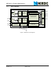
nRF24L01+ Product Specification 1.2 Block diagram RF Transmitter PA Baseband TX Filter CSN TX FIFOs GFSK Modulator SPI LNA ANT2 Radio Control VDD_PA DVDD Power Management IREF RF Synthesiser VSS XC2 RX FIFOs VDD XC1 GFSK Demodulator Figure 1. nRF24L01+ block diagram Revision 1.
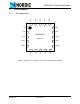
nRF24L01+ Product Specification VDD VSS IREF Pin assignment DVDD 2.1 Pin Information VSS 2 20 19 18 17 16 CE 1 15 VDD CSN 2 14 VSS 13 ANT2 nRF24L01+ SCK 3 QFN20 4X4 5 11 VDD_PA 6 7 8 9 10 XC1 MISO XC2 ANT1 VSS 12 VDD 4 IRQ MOSI Figure 2. nRF24L01+ pin assignment (top view) for the QFN20 4x4 package Revision 1.
nRF24L01+ Product Specification 2.
nRF24L01+ Product Specification 3 Absolute maximum ratings Note: Exceeding one or more of the limiting values may cause permanent damage to nRF24L01+. Operating conditions Supply voltages VDD VSS Input voltage VI Output voltage VO Total Power Dissipation PD (TA=85°C) Temperatures Operating Temperature Storage Temperature Minimum Maximum Units -0.3 3.6 0 V V -0.3 5.25 V VSS to VDD VSS to VDD -40 -40 Table 2. Absolute maximum ratings Revision 1.
nRF24L01+ Product Specification 4 Operating conditions Symbol Parameter (condition) VDD Supply voltage Supply voltage if input signals >3.6V VDD TEMP Operating Temperature Notes Table 3. Operating conditions Revision 1.0 Page 13 of 78 Min. 1.9 2.7 -40 Typ. 3.0 3.0 +27 Max. Units 3.6 V 3.
nRF24L01+ Product Specification 5 Electrical specifications Conditions: VDD = +3V, VSS = 0V, TA = - 40ºC to + 85ºC 5.1 Power consumption Symbol IVDD_PD IVDD_ST1 IVDD_ST2 IVDD_SU IVDD_TX0 IVDD_TX6 IVDD_TX12 IVDD_TX18 IVDD_AVG IVDD_TXS IVDD_2M IVDD_1M IVDD_250 IVDD_RXS Parameter (condition) Notes Idle modes Supply current in power down a Supply current in standby-I mode Supply current in standby-II mode Average current during 1.
nRF24L01+ Product Specification 5.2 General RF conditions Symbol fOP PLLres fXTAL Δf250 Δf1M Δf2M RGFSK Parameter (condition) Notes a Operating frequency PLL Programming resolution Crystal frequency Frequency deviation @ 250kbps Frequency deviation @ 1Mbps Frequency deviation @ 2Mbps b Air Data rate c FCHANNEL 1M Non-overlapping channel spacing @ 250kbps/ 1Mbps c FCHANNEL 2M Non-overlapping channel spacing @ 2Mbps Min. 2400 Typ. Max.
nRF24L01+ Product Specification 5.4 Receiver operation Datarate Symbol RXmax RXSENS RXSENS RXSENS 2Mbps 1Mbps 250kbps Parameter (condition) Notes Min. Maximum received signal at <0.1% BER Sensitivity (0.1%BER) @2Mbps Sensitivity (0.1%BER) @1Mbps Sensitivity (0.1%BER) @250kbps Typ. Max. Units 0 dBm -82 dBm -85 dBm -94 dBm Table 7. RX Sensitivity Datarate Symbol Parameter (condition) Notes Min.
nRF24L01+ Product Specification Datarate 2Mbps Symbol C/ICO C/I1ST C/I2ND C/I3RD C/INth C/INth 1Mbps C/ICO C/I1ST C/I2ND C/I3RD C/INth C/INth 250kbps C/ICO C/I1ST C/I2ND C/I3RD C/INth C/INth Parameter (condition) C/I Co-channel (Modulated carrier) Notes Min.
nRF24L01+ Product Specification Datarate Symbol Parameter (condition) Notes Min. Typ. Max.
nRF24L01+ Product Specification 5.5 Crystal specifications Symbol Fxo ΔF C0 Ls CL ESR Parameter (condition) Crystal Frequency Tolerance Equivalent parallel capacitance Equivalent serial inductance Load capacitance Equivalent Series Resistance Notes Min. Typ. 16 ab c 8 1.5 30 12 Max. ±60 7.0 16 100 Units MHz ppm pF mH pF Ω a. Frequency accuracy including; tolerance at 25ºC, temperature drift, aging and crystal loading. b.
nRF24L01+ Product Specification 5.6 DC characteristics Symbol VIH VIL Parameter (condition) HIGH level input voltage LOW level input voltage Notes Min. 0.7VDD VSS Typ. Max. Units V 0.3VDD V 5.25a a. If the input signal >3.6V, the VDD of the nRF24L01+ must be between 2.7V and 3.3V (3.0V±10%) Table 12. Digital input pin Symbol VOH VOL Parameter (condition) HIGH level output voltage (IOH=-0.25mA) LOW level output voltage (IOL=0.25mA) Notes Min. VDD -0.3 Typ. Max. VDD 0.3 Units V V Max.
nRF24L01+ Product Specification 6 Radio Control This chapter describes the nRF24L01+ radio transceiver’s operating modes and the parameters used to control the radio. The nRF24L01+ has a built-in state machine that controls the transitions between the chip’s operating modes. The state machine takes input from user defined register values and internal signals. 6.1 Operational Modes You can configure the nRF24L01+ in power down, standby, RX or TX mode. This section describes these modes in detail. 6.1.
nRF24L01+ Product Specification . Legend: Undefined Undefined Undefined VDD >= 1.
nRF24L01+ Product Specification 6.1.3.2 Standby-II mode In standby-II mode extra clock buffers are active and more current is used compared to standby-I mode. nRF24L01+ enters standby-II mode if CE is held high on a PTX device with an empty TX FIFO. If a new packet is uploaded to the TX FIFO, the PLL immediately starts and the packet is transmitted after the normal PLL settling delay (130µs). Register values are maintained and the SPI can be activated during both standby modes.
nRF24L01+ Product Specification 6.1.6 Operational modes configuration The following table (Table 15.) describes how to configure the operational modes. RX mode TX mode PWR_UP register 1 1 PRIM_RX register 1 0 TX mode 1 0 Standby-II Standby-I Power Down 1 1 0 0 - Mode CE input pin FIFO state 1 1 Data in TX FIFOs. Will empty all levels in TX FIFOsa. Minimum 10µs Data in TX FIFOs.Will empty one high pulse level in TX FIFOsb. 1 TX FIFO empty. 0 No ongoing packet transmission. - a.
nRF24L01+ Product Specification 6.2 Air data rate The air data rate is the modulated signaling rate the nRF24L01+ uses when transmitting and receiving data. It can be 250kbps, 1Mbps or 2Mbps. Using lower air data rate gives better receiver sensitivity than higher air data rate. But, high air data rate gives lower average current consumption and reduced probability of on-air collisions. The air data rate is set by the RF_DR bit in the RF_SETUP register.
nRF24L01+ Product Specification 6.5 PA control The PA (Power Amplifier) control is used to set the output power from the nRF24L01+ power amplifier. In TX mode PA control has four programmable steps, see Table 17. The PA control is set by the RF_PWR bits in the RF_SETUP register. SPI RF-SETUP RF output power (RF_PWR) 11 0dBm 10 -6dBm 01 -12dBm 00 -18dBm DC current consumption 11.3mA 9.0mA 7.5mA 7.0mA Conditions: VDD = 3.0V, VSS = 0V, TA = 27ºC, Load impedance = 15Ω+j88Ω. Table 17.
nRF24L01+ Product Specification 7 Enhanced ShockBurst™ Enhanced ShockBurst™ is a packet based data link layer that features automatic packet assembly and timing, automatic acknowledgement and retransmissions of packets. Enhanced ShockBurst™ enables the implementation of ultra low power and high performance communication with low cost host microcontrollers.
nRF24L01+ Product Specification 7.3 Enhanced Shockburst™ packet format The format of the Enhanced ShockBurst™ packet is described in this section. The Enhanced ShockBurst™ packet contains a preamble, address, packet control, payload and CRC field. Figure 5. shows the packet format with MSB to the left. P re a m b le 1 b y te A d d re s s 3 -5 b y te P a c k e t C o n tro l F ie ld 9 b it P a y lo a d 0 - 3 2 b y te C R C 1 -2 b y te Figure 5.
nRF24L01+ Product Specification 7.3.3.1 Payload length This 6 bit field specifies the length of the payload in bytes. The length of the payload can be from 0 to 32 bytes. Coding: 000000 = 0 byte (only used in empty ACK packets.) 100000 = 32 byte, 100001 = Don’t care. This field is only used if the Dynamic Payload Length function is enabled. 7.3.3.2 PID (Packet identification) The 2 bit PID field is used to detect if the received packet is new or retransmitted.
nRF24L01+ Product Specification With the DPL feature the nRF24L01+ can decode the payload length of the received packet automatically instead of using the RX_PW_Px registers. The MCU can read the length of the received payload by using the R_RX_PL_WID command. Note: Always check if the packet width reported is 32 bytes or shorter when using the R_RX_PL_WID command. If its width is longer than 32 bytes then the packet contains errors and must be discarded. Discard the packet by using the Flush_RX command.
nRF24L01+ Product Specification 7.3.6 Automatic packet assembly The automatic packet assembly assembles the preamble, address, packet control field, payload and CRC to make a complete packet before it is transmitted.
nRF24L01+ Product Specification 7.3.7 Automatic packet disassembly After the packet is validated, Enhanced ShockBurst™ disassembles the packet and loads the payload into the RX FIFO, and asserts the RX_DR IRQ.
nRF24L01+ Product Specification 7.4 Automatic packet transaction handling Enhanced ShockBurst™ has two functions for automatic packet transaction handling; auto acknowledgement and auto re-transmit. 7.4.1 Auto acknowledgement Auto acknowledgment is a function that automatically transmits an ACK packet to the PTX after it has received and validated a packet. The auto acknowledgement function reduces the load of the system MCU and can remove the need for dedicated SPI hardware.
nRF24L01+ Product Specification • • • Auto Retransmit Delay (ARD) has elapsed. No address match within 250µs (or 500µs in 250kbps mode). After received packet (CRC correct or not). nRF24L01+ asserts the TX_DS IRQ when the ACK packet is received. nRF24L01+ enters standby-I mode if there is no more untransmitted data in the TX FIFO and the CE pin is low. If the ACK packet is not received, nRF24L01+ goes back to TX mode after a delay defined by ARD and retransmits the data.
nRF24L01+ Product Specification 7.5 Enhanced ShockBurst flowcharts This section contains flowcharts outlining PTX and PRX operation in Enhanced ShockBurst™. 7.5.1 PTX operation The flowchart in Figure 10. outlines how a nRF24L01+ configured as a PTX behaves after entering standby-I mode.
nRF24L01+ Product Specification Activate PTX mode by setting the CE pin high. If there is a packet present in the TX FIFO the nRF24L01+ enters TX mode and transmits the packet. If Auto Retransmit is enabled, the state machine checks if the NO_ACK flag is set. If it is not set, the nRF24L01+ enters RX mode to receive an ACK packet. If the received ACK packet is empty, only the TX_DS IRQ is asserted.
nRF24L01+ Product Specification 7.5.2 PRX operation The flowchart in Figure 11. outlines how a nRF24L01+ configured as a PRX behaves after entering standby-I mode.
nRF24L01+ Product Specification RX FIFO and the RX_DR IRQ is asserted. If the last received packet from the transmitter is acknowledged with an ACK packet with payload, the TX_DS IRQ indicates that the PTX received the ACK packet with payload. If the No_ACK flag is not set in the received packet, the PRX enters TX mode. If there is a pending payload in the TX FIFO it is attached to the ACK packet. After the ACK packet is transmitted, the nRF24L01+ returns to RX mode.
nRF24L01+ Product Specification 7.6 MultiCeiver™ MultiCeiver™ is a feature used in RX mode that contains a set of six parallel data pipes with unique addresses. A data pipe is a logical channel in the physical RF channel. Each data pipe has its own physical address (data pipe address) decoding in the nRF24L01+. PTX3 PTX4 PTX2 2 Da ta P 5 Pi pe PTX6 Da ta e3 pe Pi Data Pip Data ta Da PTX1 Pipe 4 PTX5 ipe 1 Data P 0 ipe PRX Frequency Channel N Figure 12.
nRF24L01+ Product Specification Each pipe can have up to a 5 byte configurable address. Data pipe 0 has a unique 5 byte address. Data pipes 1-5 share the four most significant address bytes. The LSByte must be unique for all six pipes. Figure 13. is an example of how data pipes 0-5 are addressed.
nRF24L01+ Product Specification 3 6A 5B 4B B6A3 5 B3B 0x 3B4B B 0x R: DD _P0: _A TX ADDR _ RX PTX3 TX RX _AD _A DR DD : R_ P0 0x :0 B3 xB B4 3B B5 4B B6 5B 0F 60 F The PRX, using MultiCeiver™ and Enhanced ShockBurst™, receives packets from more than one PTX. To ensure that the ACK packet from the PRX is transmitted to the correct PTX, the PRX takes the data pipe address where it received the packet and uses it as the TX address when transmitting the ACK packet. Figure 14.
nRF24L01+ Product Specification 7.7 Enhanced ShockBurst™ timing This section describes the timing sequence of Enhanced ShockBurst™ and how all modes are initiated and operated. The Enhanced ShockBurst™ timing is controlled through the Data and Control interface. The nRF24L01+ can be set to static modes or autonomous modes where the internal state machine controls the events. Each autonomous mode/sequence ends with an interrupt at the IRQ pin.
nRF24L01+ Product Specification TESB Cycle >10us TUL PTX SPI 130us TIRQ TOA IRQ: TX DS UL PTX CE PTX IRQ PTX MODE PRX MODE Standby 1 Standby 1 PLL Lock PLL Lock TX RX PLL Lock RX Standby 1 PLL Lock TX PLL Lock TACK 130us RX PRX IRQ PRX CE PRX SPI IRQ:RX DR/DL 130us 130us TIRQ Figure 16. Timing of Enhanced ShockBurst™ for one packet upload (2Mbps) In Figure 16. the transmission and acknowledgement of a packet is shown.
nRF24L01+ Product Specification In Figure 17. the PTX timing of a packet transmission is shown when the first ACK packet is lost. To see the complete transmission when the ACK packet fails see Figure 20. on page 46. >10us TUL PTX SPI ARD 130us TOA 130us PLL Lock TX PLL Lock 250us max 130us UL PTX CE PTX IRQ PTX MODE Standby I RX Standby II PLL Lock TX Figure 17. Timing of Enhanced ShockBurst™ when the first ACK packet is lost (2Mbps) Revision 1.
nRF24L01+ Product Specification 7.8 Enhanced ShockBurst™ transaction diagram This section describes several scenarios for the Enhanced ShockBurst™ automatic transaction handling. The call outs in this section’s figures indicate the IRQs and other events. For MCU activity the event may be placed at a different timeframe. Note: The figures in this section indicate the earliest possible download (DL) of the packet to the MCU and the latest possible upload (UL) of payload to the transmitter. 7.8.
nRF24L01+ Product Specification 7.8.2 Single transaction with a lost packet Figure 19. is a scenario where a retransmission is needed due to loss of the first packet transmit. After the packet is transmitted, the PTX enters RX mode to receive the ACK packet. After the first transmission, the PTX waits a specified time for the ACK packet, if it is not in the specific time slot the PTX retransmits the packet as shown in Figure 19. MCU PTX UL IRQ Packet PID=1 lost during transmission No address detected.
nRF24L01+ Product Specification 7.8.4 Single transaction with ACK payload packet Figure 21. is a scenario of the basic auto acknowledgement with payload. After the packet is transmitted by the PTX and received by the PRX the ACK packet with payload is transmitted from the PRX to the PTX. The RX_DR IRQ is asserted after the packet is received by the PRX, whereas on the PTX side the TX_DS IRQ is asserted when the ACK packet is received by the PTX.
nRF24L01+ Product Specification 7.8.6 Two transactions with ACK payload packet and the first ACK packet lost MCU PTX UL1 UL2 130us PTX TX:PID=1 DL IRQ UL3 No address detected.
nRF24L01+ Product Specification 7.9 Compatibility with ShockBurst™ You must disable Enhanced ShockBurst™ for backward compatibility with the nRF2401A, nRF2402, nRF24E1 and nRF24E2. Set the register EN_AA = 0x00 and ARC = 0 to disable Enhanced ShockBurst™. In addition, the nRF24L01+ air data rate must be set to 1Mbps or 250kbps. 7.9.1 ShockBurst™ packet format Figure 25. shows the packet format with MSB to the left. Preamble 1 byte Address 3-5 byte Payload 1 - 32 byte CRC 1-2 byte Figure 25.
nRF24L01+ Product Specification 8 Data and Control Interface The data and control interface gives you access to all the features in the nRF24L01+.
nRF24L01+ Product Specification Command name R_REGISTER W_REGISTER Command # Data bytes word (binary) 000A AAAA 1 to 5 LSByte first 001A AAAA 1 to 5 LSByte first R_RX_PAYLOAD 0110 0001 1 to 32 LSByte first W_TX_PAYLOAD 1010 0000 FLUSH_TX FLUSH_RX 1110 0001 1110 0010 1 to 32 LSByte first 0 0 REUSE_TX_PL 1110 0011 0 R_RX_PL_WIDa 0110 0000 1 W_ACK_PAYLOADa 1010 1PPP 1 to 32 LSByte first W_TX_PAYLOAD_NO ACKa NOP 1011 0000 1 to 32 LSByte first 0 1111 1111 Operation Read command and status
nRF24L01+ Product Specification Note: The 3 bit pipe information in the STATUS register is updated during the IRQ pin high to low transition. The pipe information is unreliable if the STATUS register is read during an IRQ pin high to low transition. 8.3.2 SPI timing SPI operation and timing is shown in Figure 26. to Figure 28. and in Table 22. to Table 27.. nRF24L01+ must be in a standby or power down mode before writing to the configuration registers. In Figure 26. to Figure 28.
nRF24L01+ Product Specification Figure 29. shows the Rpull and Cload that are referenced in Table 22. to Table 27. Vdd Rpull External nRF24L01+ pin Cload Figure 29. Rpull and Cload Symbol Tdc Tdh Tcsd Tcd Tcl Tch Fsck Tr,Tf Tcc Tcch Tcwh Tcdz Parameters Data to SCK Setup SCK to Data Hold CSN to Data Valid SCK to Data Valid SCK Low Time SCK High Time SCK Frequency SCK Rise and Fall CSN to SCK Setup SCK to CSN Hold CSN Inactive time CSN to Output High Z Min.
nRF24L01+ Product Specification Symbol Tcch Tcwh Tcdz Parameters SCK to CSN Hold CSN Inactive time CSN to Output High Z Min. 2 50 Max 42 Units ns ns ns Table 23. SPI timing parameters (Cload = 10pF) Symbol Tdc Tdh Tcsd Tcd Tcl Tch Fsck Tr,Tf Tcc Tcch Tcwh Tcdz Parameters Data to SCK Setup SCK to Data Hold CSN to Data Valid SCK to Data Valid SCK Low Time SCK High Time SCK Frequency SCK Rise and Fall CSN to SCK Setup SCK to CSN Hold CSN Inactive time CSN to Output High Z Min.
nRF24L01+ Product Specification Symbol Tdc Tdh Tcsd Tcd Tcl Tch Fsck Tr,Tf Tcc Tcch Tcwh Tcdz Parameters Data to SCK Setup SCK to Data Hold CSN to Data Valid SCK to Data Valid SCK Low Time SCK High Time SCK Frequency SCK Rise and Fall CSN to SCK Setup SCK to CSN Hold CSN Inactive time CSN to Output High Z Min. 2 2 Max 75 85 40 40 0 5 100 2 2 50 75 Units ns ns ns ns ns ns MHz ns ns ns ns ns Table 26.
nRF24L01+ Product Specification You can write to the TX FIFO using these three commands; W_TX_PAYLOAD and W_TX_PAYLOAD_NO_ACK in PTX mode and W_ACK_PAYLOAD in PRX mode. All three commands provide access to the TX_PLD register (see Table 28. on page 63. for details of this register). The RX FIFO can be read by the command R_RX_PAYLOAD in PTX and PRX mode. This command provides access to the RX_PLD register. The payload in TX FIFO in a PTX is not removed if the MAX_RT IRQ is asserted.
nRF24L01+ Product Specification 9 Register Map You can configure and control the radio by accessing the register map through the SPI. 9.1 Register map table All undefined bits in the table below are redundant. They are read out as '0'. Note: Addresses 18 to 1B are reserved for test purposes, altering them makes the chip malfunction.
nRF24L01+ Product Specification Address (Hex) 03 04 Mnemonic Bit ERX_P1 ERX_P0 1 0 Reset Value 1 1 SETUP_AW Reserved AW 7:2 1:0 000000 11 SETUP_RETR ARDa 7:4 0000 ARC 3:0 0011 RF_CH Reserved RF_CH 7 6:0 0 0000010 RF_SETUP CONT_WAVE Reserved RF_DR_LOW 7 6 5 0 0 0 PLL_LOCK RF_DR_HIGH 4 3 0 1 05 06 Revision 1.0 Type Description R/W Enable data pipe 1. R/W Enable data pipe 0.
nRF24L01+ Product Specification Address (Hex) 07 08 Bit RF_PWR 2:1 Obsolete 0 Reset Value 11 Type Reserved RX_DR 7 6 0 0 R/W R/W TX_DS 5 0 R/W MAX_RT 4 0 R/W RX_P_NO 3:1 111 R TX_FULL 0 0 R OBSERVE_TX PLOS_CNT 7:4 0 R ARC_CNT 3:0 0 R RPD Reserved RPD 7:1 0 000000 0 R R RX_ADDR_P0 39:0 0xE7E7E 7E7E7 Revision 1.
nRF24L01+ Product Specification Address (Hex) 0B Mnemonic Bit RX_ADDR_P1 39:0 0C RX_ADDR_P2 7:0 0D RX_ADDR_P3 7:0 0E RX_ADDR_P4 7:0 0F RX_ADDR_P5 7:0 10 TX_ADDR 39:0 0xE7E7E 7E7E7 R/W Transmit address. Used for a PTX device only. (LSByte is written first) Set RX_ADDR_P0 equal to this address to handle automatic acknowledge if this is a PTX device with Enhanced ShockBurst™ enabled. See page 75.
nRF24L01+ Product Specification Address (Hex) Mnemonic Bit RX_PW_P3 5:0 Reset Value 0 RX_PW_P4 Reserved RX_PW_P4 7:6 5:0 00 0 R/W Only '00' allowed R/W Number of bytes in RX payload in data pipe 4 (1 to 32 bytes). 0 Pipe not used 1 = 1 byte … 32 = 32 bytes RX_PW_P5 Reserved RX_PW_P5 7:6 5:0 00 0 R/W Only '00' allowed R/W Number of bytes in RX payload in data pipe 5 (1 to 32 bytes).
nRF24L01+ Product Specification Address (Hex) N/A Mnemonic Bit ACK_PLD 255:0 Reset Value X N/A TX_PLD 255:0 X W N/A RX_PLD 255:0 X R 1C DYNPD Reserved DPL_P5 7:6 5 0 0 DPL_P4 4 0 DPL_P3 3 0 Revision 1.0 Type Description W Written by separate SPI command ACK packet payload to data pipe number PPP given in SPI command. Used in RX mode only. Maximum three ACK packet payloads can be pending. Payloads with same PPP are handled first in first out.
nRF24L01+ Product Specification Address (Hex) 1D Mnemonic Bit DPL_P2 2 Reset Value 0 DPL_P1 1 0 DPL_P0 0 0 FEATURE Reserved EN_DPL EN_ACK_PAYd EN_DYN_ACK 7:3 2 1 0 0 0 0 0 Type Description R/W Enable dynamic payload length data pipe 2. (Requires EN_DPL and ENAA_P2) R/W Enable dynamic payload length data pipe 1. (Requires EN_DPL and ENAA_P1) R/W Enable dynamic payload length data pipe 0.
nRF24L01+ Product Specification 10 Peripheral RF Information This chapter describes peripheral circuitry and PCB layout requirements that are important for achieving optimum RF performance from the nRF24L01+. 10.1 Antenna output The ANT1 and ANT2 output pins provide a balanced RF output to the antenna. The pins must have a DC path to VDD_PA, either through a RF choke or through the center point in a balanced dipole antenna. A load of 15Ω+j88Ω is recommended for maximum output power (0dBm).
nRF24L01+ Product Specification XO_OUT Buffer: Sine to full swing Amplitude controlled current source Current starved inverter: XOSC core Vdd Vdd Rbias Vss Vss ESD ESD XC1 XC2 Figure 31. Principle of crystal oscillator The nRF24L01+ crystal oscillator is amplitude regulated. It is recommended to use an input signal larger than 0.4V-peak to achieve low current consumption and good signal-to-noise ratio when using an external clock.
nRF24L01+ Product Specification 11 Application example nRF24L01+ with single ended matching network crystal, bias resistor, and decoupling capacitors. C7 33nF 0402 C8 1nF 0402 1 2 3 4 5 CE CSN SCK MOSI MISO nRF24L01+ 15 14 13 12 11 VDD VSS ANT2 ANT1 VDD_PA IRQ VDD VSS XC2 XC1 CE CSN SCK MOSI MISO U1 VSS DVDD VDD VSS IREF C9 10nF 0402 R2 22K 0402 20 19 18 17 16 VDD C5 L3 L1 8.2nH 0402 50ohm, R 3.9nH 0402 1.5pF 0402 C6 1.0pF 0402 L2 2.7nH 0402 6 7 8 9 10 NRF24L01 IRQ C3 2.
nRF24L01+ Product Specification Part a 22pF 22pFa 2.2nF 4.7pF 1.5pF 1,0pF 33nF 1nF 10nF 8,2nH 2.7nH 3,9nH Not mountedb 22kΩ nRF24L01+ 16MHz Designator C1 C2 C3 C4 C5 C6 C7 C8 C9 L1 L2 L3 R1 R2 U1 X1 Footprint 0402 0402 0402 0402 0402 0402 0402 0402 0402 0402 0402 0402 0402 0402 QFN20 4x4 Description NPO, +/- 2% NPO, +/- 2% X7R, +/- 10% NPO, +/- 0.25pF NPO, +/- 0.1pF NPO, +/- 0.
nRF24L01+ Product Specification + Figure 33. Top overlay (nRF24L01+ RF layout with single ended connection to PCB antenna and 0402 size passive components) Figure 34. Top layer (nRF24L01+ RF layout with single ended connection to PCB antenna and 0402 size passive components) Revision 1.
nRF24L01+ Product Specification Figure 35. Bottom layer (nRF24L01+ RF layout with single ended connection to PCB antenna and 0402 size passive components The nest figure (Figure 36., Figure 37. and Figure 38.) is for the SMA output to have a board for direct measurements at a 50Ω SMA connector. Figure 36. Top Overlay (Module with OFM crystal and SMA connector) Revision 1.
nRF24L01+ Product Specification Figure 37. Top Layer (Module with OFM crystal and SMA connector) Figure 38. Bottom Layer (Module with OFM crystal and SMA connector) Revision 1.
nRF24L01+ Product Specification 12 Mechanical specifications nRF24L01+ uses the QFN20 4x4 package, with matt tin plating. Revision 1.
nRF24L01+ Product Specification Package Type Saw QFN20 (4x4 mm) Min. Typ. Max A 0.80 0.85 0.95 A1 A3 0.00 0.02 0.20 0.05 REF. K 0.20 min. D/E e D2/E2 2.50 4.0 0.5 BSC 2.60 2.70 BSCa a. BSC: Basic Spacing between Centers, ref. JEDEC standard 95, page 4.17-11/A Figure 39. nRF24L01+ Package Outline Revision 1.0 Page 72 of 78 L 0.35 0.40 0.45 L1 0.15 max b 0.18 0.25 0.
nRF24L01+ Product Specification 13 Ordering information 13.1 Package marking n 2 Y 13.2 R F A 4 L 0 1 Y W W L X + L Abbreviations Abbreviation nRF A X YY WW LL Definition Fixed text Variable Build Code, that is, unique code for production sites, package type and test platform “X" grade, that is, Engineering Samples (optional) 2 digit Year number 2 digit Week number 2 letter wafer lot number code 13.3 Product options 13.3.
nRF24L01+ Product Specification 14 Glossary of Terms Term ACK ACS AGC ART CD CE CLK CRC CSN ESB GFSK IM IRQ ISM LNA LSB LSByte Mbps MCU MISO MOSI MSB MSByte PCB PID PLD PRX PTX PWR_DWN PWR_UP RoHS RPD RX RX_DR SPI TX TX_DS Description Acknowledgement Adjacent Channel Selectivity Automatic Gain Control Auto Re-Transmit Carrier Detect Chip Enable Clock Cyclic Redundancy Check Chip Select NOT Enhanced ShockBurst™ Gaussian Frequency Shift Keying Intermodulation Interrupt Request Industrial-Scientific-Medical
nRF24L01+ Product Specification Appendix A - Enhanced ShockBurst™ - Configuration and communication example Enhanced ShockBurst™ transmitting payload 1. 2. 3. 4. 5. 6. 7. Set the configuration bit PRIM_RX low. When the application MCU has data to transmit, clock the address for the receiving node (TX_ADDR) and payload data (TX_PLD) into nRF24L01+ through the SPI. The width of TX-payload is counted from the number of bytes written into the TX FIFO from the MCU.
nRF24L01+ Product Specification Enhanced ShockBurst™ receive payload 1. 2. 3. 4. 5. 6. 7. 8. Select RX by setting the PRIM_RX bit in the CONFIG register to high. All data pipes that receive data must be enabled (EN_RXADDR register), enable auto acknowledgement for all pipes running Enhanced ShockBurst™ (EN_AA register), and set the correct payload widths (RX_PW_Px registers). Set up addresses as described in item 2 in the Enhanced ShockBurst™ transmitting payload example above.
nRF24L01+ Product Specification Appendix B - Configuration for compatibility with nRF24XX How to setup nRF24L01+ to receive from an nRF2401/nRF2402/nRF24E1/nRF24E2: 1. 2. 3. 4. 5. 6. 7. 8. Use the same CRC configuration as the nRF2401/nRF2402/nRF24E1/nRF24E2. Set the PWR_UP and PRIM_RX bit to 1. Disable auto acknowledgement on the data pipe that is addressed. Use the same address width as the PTX device. Use the same frequency channel as the PTX device.
nRF24L01+ Product Specification Appendix C - Constant carrier wave output for testing The output power of a radio is a critical factor for achieving wanted range. Output power is also the first test criteria needed to qualify for all telecommunication regulations. Configuration 1. 2. 3. 4. 5. 6. Set PWR_UP = 1 and PRIM_RX = 0 in the CONFIG register. Wait 1.5ms PWR_UP->standby. In the RF register set: X CONT_WAVE = 1. X PLL_LOCK = 1. X RF_PWR. Set the wanted RF channel. Set CE high.