OPERATOR MANUAL BIT 4886 DIGITAL INTERFACE CARD WITH GPIB AND RS 232 CAPABILITY MODEL KEPCO INC. An ISO 9001 Company. BIT 4886 INTERFACE CARD IMPORTANT NOTES: 1) This manual is valid for the following Firmware Versions: FIRMWARE VERSION NOTE. 2) A Change Page may be included at the end of the manual. All applicable changes and revision number changes are documented with reference to the equipment serial numbers.
TABLE OF CONTENTS SECTION PAGE SECTION 1 - INTRODUCTION 1.1 1.2 1.2.1 1.2.2 1.3 1.3.1 Scope of Manual ..................................................................................................................................... 1-1 General Description................................................................................................................................. 1-1 Measurements .......................................................................................................
TABLE OF CONTENTS SECTION PAGE 4.6.3 SCPI Subsystem Command/Query Structure................................................................................... 4-14 4.6.3.1 Initiate Subsystem....................................................................................................................... 4-15 4.6.3.2 Measure Subsystem ................................................................................................................... 4-15 4.6.3.
TABLE OF CONTENTS SECTION PAGE APPENDIX B - SCPI COMMAND/QUERY DEFINITIONS B.1 B.2 B.3 B.4 B.5 B.6 B.7 B.8 B.9 B.10 B.11 B.12 B.13 B.14 B.15 B.16 B.17 B.18 B.19 B.20 B.21 B.22 B.23 B.24 B.25 B.26 B.27 B.28 B.29 B.30 B.31 B.32 B.33 B.34 B.35 B.36 B.37 B.38 B.39 B.40 B.41 B.42 B.43 B.44 B.45 B.46 B.47 B.48 B.49 B.50 B.51 B.52 B.53 B.54 Introduction............................................................................................................................................. Numerical Values ..
TABLE OF CONTENTS SECTION B.55 B.56 B.57 B.58 B.59 B.60 B.61 B.62 B.63 B.64 B.65 B.66 B.67 B.68 B.69 B.70 B.71 B.72 B.73 B.74 B.75 B.76 B.77 B.78 B.79 B.80 B.81 B.82 B.83 B.84 B.85 B.86 B.87 B.88 B.89 B.90 B.91 B.92 iv PAGE [SOURce:]CURRent[:LEVel]TRIGgered[:AMPlitude] Command............................................................ [SOURce:]CURRent[:LEVel]TRIGgered[:AMPlitude]? Query.................................................................
LIST OF FIGURES FIGURE 1-1 2-1 2-2 2-3 2-4 3-1 3-2 3-3 3-4 4-1 4-2 4-3 4-4 4-5 4-6 4-7 A-1 B-1 B-2 B-3 B-4 B-5 B-6 B-7 B-8 TITLE PAGE Remotely Controlled Power Supply Configurations Using Kepco Products................................................ viii BIT 4886 Switch Locations ......................................................................................................................... 2-2 Installation of Model BIT 4886 into BOP ............................................................
LIST OF TABLES TABLE 1-1 1-2 1-3 1-4 1-5 2-1 2-2 2-3 2-4 2-5 3-1 3-2 3-3 3-4 4-1 4-2 4-3 4-4 4-5 4-6 A-1 A-2 A-3 B-1 B-2 B-3 B-4 B-5 B-6 vi TITLE PAGE Applicability of BIT 4886 Cards to Specific BOP Models ........................................................................... 1-1 BOP Voltage Specifications with BIT 4886 Installed .................................................................................. 1-2 BOP Current Specifications with BIT 4886 Installed ................................
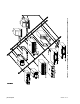
(vii Blank)/viii BIT4886 120413 FIGURE 1-1.
SECTION 1 - INTRODUCTION 1.1 SCOPE OF MANUAL This manual contains instructions for the installation, operation and maintenance of the BIT 4886 Interface Card manufactured by Kepco, Inc, Flushing, NY, U.S.A. 1.2 GENERAL DESCRIPTION The Kepco BIT Card Series were designed as an accessory for the Kepco BOP series bipolar power supplies. The BIT 4886 card makes it possible to control the BOP output by means of digital input signals via the IEEE 488.2 bus using SCPI commands (see Figure 1-1).
1.2.2 ENHANCED OPERATION The BIT 4886 card includes the following enhanced operation features: a) advanced control over the way the unit responds to errors (PAR. 4.7.1), b) advanced limit channel control for applications such as battery, photocell, and large inductor applications (see PAR. 4.7.2) and c) ability to save system settings (PAR. 4.7.3). 1.3 SPECIFICATIONS For voltage and current accuracy specifications of BOP Models with a BIT 4886 card installed, refer to Tables 1-2 and 1-3, respectively.
TABLE 1-4.
1.3.1 BIT 4882 COMPATIBILITY The BIT 4886 card complies with the SCPI 1997 standard as a member of the power supply instrument class. The Bit 4882 product complies with the 1990 version of the SCPI standard. During the years of 1990 to 1997, the SCPI consortium refined the standard, providing direction for the *RST command and indicating the differences between *RST and the single byte GPIB command of DCL and SDC.
SECTION 2 - INSTALLATION 2.1 UNPACKING AND INSPECTION The Interface Card has been thoroughly inspected and tested prior to packing and is ready for operation following installation. Unpack, saving original packing material. If any indication of damage is found, file a claim immediately with the responsible transport service. See Table 2-1 for items supplied. TABLE 2-1.
2.2.1 SET (GPIB) DEVICE ADDRESS (SEE FIGURE 2-1) The Device Address for the interface card is set by means of DIP switch S1, positions 1 through 5 (Figure 2-1). The Device Address is the permanent Listener or Talker address of the interface card on the GPIB. It is factory preset to address 6. If a different Device Address is required in your system, proceed as follows. There are 31 (1-31) possible choices (See Table 2-2). 1. Position the Interface Card as depicted in Figure 2-1. 2.
TABLE 2-2.
2.3 INSTALLATION OF INTERFACE CARD INTO THE BOP Refer to Figure 2-2 to install the BIT 4886 interface card. CAUTION: The BIT 4886 card contains ESD sensitive components. Follow all procedures in effect at your facility for handling ESD sensitive components. NOTE: Step numbers coincide with encircled numbers on Figure 2-2. Step 1. Remove a-c power to BOP by disconnecting line cord. Step 2. Remove BOP cover (see Section 5, Figure 5-1 of your BOP Instruction Manual). Step 3.
FIGURE 2-2.
2.4 INPUT/OUTPUT SIGNALS The IEEE 488 port is a 24 pin IEEE 488 connector (Figure 2-3) and conforms mechanically and electrically to the IEEE 488 standard; refer to Table 2-3 for pin assignments. Table 2-4 describes the RS 232 port pin connections. TABLE 2-3.
TABLE 2-4. RS232C PORT INPUT/OUTPUT PIN ASSIGNMENTS CONNECTOR PIN RS 232 PORT SIGNAL NAME FUNCTION 1 RTS Request To Send (protocol not used) 2 RXD Receive Data 3 TXD Transmit Data 4 LOGIC GND Logic Ground 5 LOGIC GND Logic Ground 6 CTS Clear To Send (protocol not used) TABLE 2-5. RJ45 TO DB9 ADAPTER WIRE FUNCTIONS Wire DB9 Pin Purpose Green 5 Return for pins 2 and 3. Brown 3 Carries data from the Kepco power supply to the controller.
2.5 INITIAL CHECK-OUT PROCEDURE After the BIT 4886 card has been installed per PAR. 2.3, perform the following procedure to verify that it is functioning properly. 1.
SECTION 3 - CALIBRATION NOTE: The calibration procedures below are for the purpose of recalibration and for the case where the BIT card is installed by the user. Unless otherwise noted, syntax is in SCPI. 3.1 EQUIPMENT REQUIRED The following is a listing of equipment required for calibration of the Interface Card installed in a Kepco “BOP” Series Power Supply: A. Precision digital voltmeter (DVM), minimum resolution 7 digits (suggested): B.
FIGURE 3-1. BOP POWER SUPPLY, INTERNAL CALIBRATION CONTROL LOCATIONS NOTE: ALL SENSE RESISTORS MUST BE MOUNTED ON A HEATSINK WITH A MINIMUM SURFACE AREA OF 36 SQUARE INCHES TO MAINTAIN THERMAL STABILITY DURING CALIBRATION. FIGURE 3-2.
3.3 CALIBRATION OF BIT 4886 INTERFACE CARD Calibration of the BIT 4886 card is performed using SCPI commands. The Instrument driver available at www.kepcopower.com/drivers.htm provides a graphical interface with informational displays and prompts which lead you through the calibration of the BIT 4886 card. This VISA compliant driver works with many GPIB cards from suppliers like National Instruments and Hewlett-Packard. Calibration using the graphical interface is described in PAR. 3.3.
TABLE 3-2. CALIBRATION MEASUREMENTS AND TOLERANCES - CURRENT MODEL BOP 100-1M BOP 200-1M BOP 50-2M BOP 100-2M BOP 72-3M BOP 50-4 BOP 100-4M BOP 20-5M BOP 36-6M BOP 72-6M BOP 50-8 BOP 20-10M BOP 36-12M 3-4 SENSE RESISTOR VALUE (SEE NOTE AND TABLE 3-3) 1 Ohm 1 Ohm 1 Ohm 1 Ohm 0.1 Ohm 0.1 Ohm 0.1 Ohm 0.1 Ohm 0.01 Ohm LOW CURRENT ZERO MAIN CURRENT ZERO MAIN CURRENT NOMINAL HIGH CURRENT ACCURACY LOW CURRENT NOMINAL LOW CURRENT ACCURACY CURRENT LIMIT ADJUST PAR. 3.3.1 STEP 17 PAR. 3.
TABLE 3-2. CALIBRATION MEASUREMENTS AND TOLERANCES - CURRENT (CONTINUED) SENSE RESISTOR VALUE (SEE NOTE AND TABLE 3-3) MODEL BOP 20-20M 0.001 Ohm REFER TO NOTES IF EXACT SENSE RESISTOR VALUE IS KNOWN. RSENSE SEE NOTE. LOW CURRENT ZERO MAIN CURRENT ZERO MAIN CURRENT NOMINAL HIGH CURRENT ACCURACY LOW CURRENT NOMINAL LOW CURRENT ACCURACY CURRENT LIMIT ADJUST PAR. 3.3.1 STEP 17 PAR. 3.3.1 STEP 18 PAR. 3.3.1 STEPS 19, 20 PAR. 3.3.1 STEPS 21, 23 PAR. 3.3.1 STEP 24, 25 PAR. 3.3.
3.3.1 MANUAL CALIBRATION 1. Initiate calibration by sending the SCPI command SYSTem:PASSword:CENable DEFAULT and then send CAL:STATe 1. The password (DEFAULT) has been set at the factory. If the password has been changed from DEFAULT, substitute the correct password for the unit in the SYST:PASS:CEN command. If the password has been forgotten, consult factory. If voltage calibration is not needed, proceed to step 16 for current calibration. 2.
10.Decrease the voltage output by sending CAL:DPOT -1 commands until the voltmeter reads less than the rated output. Then send CAL:DPOT 1 and verify the voltage is slightly above value specified in Table 3-1 for LOW RANGE NOMINAL. 11. Send the command CAL:DATA -10 to decrease the voltage until the voltage is less than value specified in Table 3-1 for LOW RANGE ACCURACY MAX.
19.Set the BOP to maximum positive output current by sending CAL:CURR MAX. Measure the voltage across the sense resistor using a Digital Voltmeter of at least 7 digits in accuracy. Verify the DVM reads the voltage specified in Table 3-2 for MAIN CURRENT NOMINAL. The voltage shown on the DVM should be positive; if not, reverse the leads to the DVM. 20.
If the CAL:DPOT command was used to adjust the negative output, after adjusting the negative supply output, send CAL:LCURR MAX to the unit and repeat step 26 before proceeding to step 29. 29.Set the BOP to current limit by sending CAL:CPR MAX. Continue to measure the output of the BOP. 30.Send the command CAL:DATA -10 to decrease the voltage across the sense resistor until the output voltage measured is within, or close to, the tolerance specified in Table 3-2 for CURRENT LIMIT ADJUST.
3.3.2.1 CALIBRATION BASICS CAUTION: Before performing calibration, set BOP OUTPUT to OFF and connect short across BOP output, then set OUTPUT to ON and Voltage to 10V. It is necessary to wait 10 minutes before calibrating the unit to allow for thermal stabilization. After 10 minutes, set OUTPUT to OFF and remove short from BOP output, then proceed with calibration. All adjustments are done using the six arrow buttons of the Calibration Panel (see Figure 3-4 and Table 3-4).
3.3.2.2 CALIBRATION PROCEDURE 1. Click on the Calibration Off button on the main panel (see Figure 3-4).This will open a calibration panel (see Figure 3-4 and Table 3-4) that allows calibration in either voltage or current mode. 2. The password (DEFAULT) has been set at the factory. If it has not been changed, it will be displayed in the box adjacent to the Start button on the right side of the panel.
12.At the calibration panel (Figure 3-4) click CURR to begin current calibration of the unit. Connect CALIBRATION RESISTOR! window opens. 13.Connect load (see Table 3-3) across the output of the unit and connect DVM across the load as shown in Figure 3-2. Voltage measurements must be converted to Amperes using Ohm’s law, E = IR. Click OK button to close Connect CALIBRATION RESISTOR window. 14.The test window reads LCurr ZERO and the message Adjust for ZERO R83 (Io Zero) on BOP A1 card. will be displayed.
SECTION 4 - OPERATION 4.1 GENERAL The Kepco BOP Power Supply, with an installed BIT 4886 Interface Card, may be programmed over the IEEE 488 standard communication bus (General Purpose Interface Bus, GPIB) using SCPI (Standard Commands for Programmable Instruments). SCPI provides a common language used in an automatic test system. (Refer to Table 2-3 for input/output signal allocations.) CAUTION: DO NOT repeatedly toggle the circuit breaker/switch as this may cause unit to fault.
and thus the output current (where s = sign, + or – and xxxx = the absolute value of output current). Sending VOLT sxxxx controls voltage limit (where s = sign, + or – and xxxx = the absolute value of voltage limit. 4.1.1.2 AUTOMATIC RANGE OPERATION. The BIT 4886 has low and high ranges which are changed automatically when the main channel set point is changed from a value less than the 1/4 of the units operating capability to a value that is higher than 1/4 of the operating capability.
becomes set, the unit is ready for its next command after reading back the data from the query that was added to the command string. When sending the above commands via the RS 232 bus, data flow control must be enabled (XON) for the unit to properly update flash memory. The *ESR? query is ideal to check if the previous command is complete since it returns either a 1 or 0. It is important that it be sent as a part of the same string as the command that causes a flash update.
#include #include #include #include /*Overhead for the use of a NATIONAL INSTRUMENTS gpib interface */ int unit_desc; // handle for the national instruments controller int GPIbus=0; // GPIB card 0 int adr=6; // Power Supply address char status_byte; // status byte from the power supply #define MAV 0x10 /* bit 4 of the status byte is the Message AVailable bit by 488.
drivers.htm by choosing the appropriate model and CVI configuration. The CVI Driver can not be used via the RS 232 Port. 1. Unzip the files and doubleclick on setup.exe to install the driver. The bit_mdac folder will be added to the Start - Programs folder. Doubleclick bit_mdac.exe to run the program, and refer to the visamdac.pdf in the bit_mdac folder for details about using the soft front panel. 2.
FIGURE 4-3. 4.2.2 BIT 4886 CARD INITIALIZATION USING VISA DRIVER INITIALIZATION USING SCPI COMMANDS AND GPIB PORT 1. With the BOP power off, place the five address switches to the on position (see Figure 2-1 for switch location). 2. Insure a GPIB controller is connected to the BOP via the GPIB cable. Set BOP power to OFF and set the address switches to the proper GPIB address to be used (refer to PAR 2.2.1, Figure 2-1, and Table 2-2 for addresses).
7. After the calibration has been completed, the master calibration levels can be established using the following command: CAL:COPY WORK FACT. 4.2.3 INITIALIZATION USING SCPI COMMANDS AND RS 232 PORT 1. With the BOP power off, place the five address switches to the on position (see Figure 2-1 for switch location). 2. Set BOP power to OFF and set the address switches to the proper GPIB address to be used (refer to PAR 2.2.1, Figure 2-1, and Table 2-2 for addresses).
SYST:SEC:OVERRIDE 4.3 BUILT IN TEST The BIT 4886 card is designed to perform periodic testing of itself, power up testing and commanded testing. The testing is reported to the operator both by errors placed in the SCPI error queue and by issuing audible beeps. The driver and demonstration soft panel which can be downloaded from the Kepco website at: www.kepcopower.com/drivers.htm provide an easy way to verify BIT 4886 performance. A description of the driver is included as an Adobe Acrobat ™ PDF file. 4.
4.3.3 BOP TEST The DIAG:TST? Command performs a test of the BOP instrument. The test includes the BIT 4886 internal tests of the DAC (Digital to Analog Converter), Limit and Op Amp circuits. If successful it programs the BOP in voltage mode to the positive and negative limits of the device. It also verifies the Limit operation of the unit in current mode by setting the unit for the rated maximum current delivery and verifies that the voltage limit set at one volt operates correctly.
These messages are enabled during the “handshake” cycle, with the Interface Card operating as either a Talker or a Listener. 4.5 RS232-C OPERATION The BIT 4886 card allows the BOP to be operated via an RS232-C terminal, or from a PC using a terminal emulation program. The default settings are as follows: • Baud rate: 9600 • Parity: None • Data Bits 8 • Stop Bits 1 • Echo ON • XON OFF To change echo or XON/XOFF, refer to PAR. 4.5.2. TABLE 4-3.
TABLE 4-4. IEEE 488 (GPIB) BUS DATA MODE MESSAGES MNEMONIC 4.5.1 MESSAGE DESCRIPTION COMMENTS DAB Data Byte Received or Sent END End Received or Sent EOS End of String Received or Sent RQS Request Service Sent STB Status Byte Sent SERIAL INTERFACE The serial interface behaves like the GPIB interface in that the command is parsed after receiving a control character of either a Line Feed or Carriage Return. The serial interface supports six special control characters.
FIGURE 4-4. RS 232 IMPLEMENTATION Only seven control characters (characters between 00H and 1FH) are acknowledged by the BIT 4886: • Carriage Return (CR, 0DH) • Line Feed (LF, 0AH) • Back Space (BS, 08H) • Escape (ESC, 01BH) • XON (011H) • XOFF (013H) • CAN (018H) BS deletes the last character entered, with the exception of CR or LF characters. Either the CR or LF character acts as the line terminator, initiating parsing of the ASCII data sent to the BIT 4886 by the command originator.
All non-control characters are sent via the serial port of the command originator. The control character BS is echoed as BS Space BS. Only the first control character is returned in response to either a CR LF or LF CR character sequence (see Figure 4-4). 4.5.2.1 ECHO MODE Echo mode is one method of ensuring data is transferred without errors. This mode should only be enabled when errors in operation are detected. Refer to PAR. B.76 to change the setting.
defective. If the response is PASSED, the cable is correct; remove the jumper and reconnect the cable to the computer. 4. If the loop back connector was not available and steps 1 And 3 were completed successfully, contact Kepco to obtain loop back connector P/N 195-0111 and rerun the test. If each of the above steps is completed successfully, the problem lies in the computer hardware and/or software.
ROOT : (colon) INITiate subsystem CALibrate subsystem STATus subsystem INITiate [:IMMediate] :CONTinuous CALibrate :STATus :STATus? :VOLT :LEVel (MIN | MAX, ZERO) [:DATA] val GAIN (UP | DOWN) :VPR (MIN | MAX) :CPR (MIN | MAX) :CURR :LEVel (MIN | MAX, ZERO) [:DATA] val :GAIN (UP | DOWN) :DPOT val :LCURR (MIN | MAX, ZERO) :LVOLT (MIN | MAX, ZERO) :ZERO :SAVE STATus :OPERation :CONDition? :ENABle [:EVENt]? :PRESet :QUEStionable :CONDition? :ENABle [:EVENt]? MEASure subsystem MEASure :CURRent?
4.6.3.3 [SOURCE:]VOLTAGE AND [SOURCE:]CURRENT SUBSYSTEMS These subsystems program the output voltage and current of the power supply. 4.6.3.4 OUTPUT SUBSYSTEM This subsystem enables/disables the power supply output. Voltage and current are determined by the combination of SOURCE subsystem VOLTage and CURRent commands and the load. 4.6.3.5 LIST SUBSYSTEM The LIST subsystem is used to generate transients, waveforms and execute a series of steps repeatedly.
4.6.3.5.2 OTHER REQUIRED COMMANDS VOLT:MODE LIST (PAR. B.59) or CURR:MODE LIST (PAR. B.50). These commands start the list and VOLT:MODE FIX (PAR. B.59) or CURR:MODE FIX (PAR. B.50) stop the list. LIST commands are not accepted while a list is running. If LIST:COUNT is between 1 and 255, when the count decrements to 0, the list stops and the unit automatically moves to VOLT:MODE FIXED or CURR:MODE FIXED state. To execute the list again, either VOLT:MODE LIST or CURR:MODE LIST must be sent again. 4.6.3.5.
NOTE: An alternative to using the message structure for multiple messages defined in the following paragraphs is to send each command as a separate line. In this case each command must use the full syntax shown in Appendix B. KEYWORD DATA SEPARATOR ROOT SPECIFIER DATA MESSAGE UNIT SEPARATOR MESSAGE UNIT SEPARATOR DATA DATA SEPARATOR ROOT SPECIFIER KEYWORD KEYWORD KEYWORD SEPARATOR QUERY INDICATOR MESSAGE TERMINATOR KEYWORD INITIAL ROOT SPECIFIER IS OPTIONAL :CURR:LEV 3.
4.6.4.2 KEYWORD SEPARATOR If a command has two or more keywords, adjacent keywords must be separated by a colon (:) which acts as the keyword separator (e.g., CURR:LEV:TRIG). The colon can also act as a root specifier (paragraph 4.6.4.7). 4.6.4.3 QUERY INDICATOR The question mark (?) following a keyword is a query indicator. This changes the command into a query. If there is more than one keyword in the command, the query indicator follows the last keyword. (e.g., VOLT? and MEAS:CURR?). 4.6.4.
• • carriage return (), ASCII 13 (decimal) or 0D (hex) both of the above ( ). If both are sent, the second is null and has no effect. Your GPIB interface card software will automatically send a message terminator. For example, the HP BASIC OUTPUT statement inserts after the last data byte. When binary data is exchanged, must be used. The combination terminator can be used for all data except binary data.
units separated by a colon (:) followed by a message terminator. Several message units of a program message may be separated by a semicolon (;) without repeating the root keyword. • If a program message has more than one message unit, then a colon (:) must precede the next keyword in order to set the parser back to the root (otherwise the next keyword will be taken as a subunit of the previous message unit). e.g.
/**************************************************************************/ /* Sample Program (written in C) for KEPCO power supply using */ /* National Instruments GPIB interface card */ /**************************************************************************/ #include #include "decl.
output off state. DIAG:OUTP nH (see Table 4-5) controls the limit DAC values when the output is set to OFF; n = 0 is the default. This sets both voltage and current limit channels to 0 when the output is off. n = 1 sets voltage limit to maximum when the output is off. n = 2 sets the current limit to the maximum when the output is off. Bits 2 and 3 of the hex character allow the DIAG:OFFLimit commands to establish a specific voltage limit and current limit, respectively, when the output is off.
The following statistics are a guide as to when a MEMORY PACK will occur. • Save area - Approximately 300 *SAV operations can be completed before a PACK will occur automatically. • Variable area - around 30 updates can be completed prior to an automatic PACK occurring. Variable areas also include serial number updates and password updates. • Calibration - 16 calibrations can be saved before a PACK is required.
TABLE 4-5. ENHANCED OPERATION - ERROR RESPONSE (CONTINUED) COMMAND QUERY DESCRIPTION DIAG:OFFLimit:VOLT xx (xx = decimal value) DIAG:OFFLimit:VOLT? The decimal value allows the user to establish the actual voltage limit DAC (digital to analog converter) setting when the output is off and the unit is in current mode. This variable is only used when bit 3 of the DIAG:OUTP register is set. The value is calculated using the equation: Voltage expected / Voltage max * 1.1) * 256 The DVS standard setting is 0.
TABLE 4-5. ENHANCED OPERATION - ERROR RESPONSE (CONTINUED) COMMAND DIAG:WIN xx (xx = hex value from 10 to 40)1 QUERY DIAG:WIN? (Returns window value xx (hex) DESCRIPTION Allows user to specify value in LSB’s for error window used for detection of output voltage or output current measurement errors (default = 32). Error window value can only be set between 16 (10 Hex) and 64 (40 Hex) using one two-digit hex character (xx)1. Query returns 2-digit hex character xx.
Tory, MASTer, FIRst. Source refers to the calibration area that is to be copied, destination to the area that the calibration will be copied into. The Master calibration should never be overwritten. Factory, Master, and First are set to the same values when a BIT 4886 card is factory-installed in a BOP power supply. The Working calibration is the active calibration. Each time a CAL:SAV is executed, the values are saved in the Working (active) area.
APPENDIX A - SCPI COMMON COMMAND/QUERY DEFINITIONS A.1 INTRODUCTION This appendix defines the SCPI common commands and queries used with the BIT 4886 Interface Card. Common commands and queries are preceded by an asterisk (*) and are defined and explained in paragraphs A.2 through A.17, arranged in alphabetical order. Table A-1 provides a quick reference of all SCPI common commands and queries used in the Interface Card. TABLE A-1. IEEE 488.2 COMMAND/QUERY INDEX A.2 COMMAND PAR. COMMAND PAR. *CLS A.
A.4 *ESE? — STANDARD EVENT STATUS ENABLE QUERY Syntax: *ESE? *ESE? Return value: Integer> value per Table A-2. Description: Returns the mask stored in the Standard Event Status Enable Register. Contents of Standard Event Status Enable register (*ESE) determine which bits of Standard Event Status register (*ESR) are enabled, allowing them to be summarized in the Status Byte register (*STB).
A.7 *OPC — OPERATION COMPLETE COMMAND Syntax: *OPC *OPC Description: Causes power supply to set status bit 0 (Operation Complete) when pending operations are complete This command sets Standard Event Status Register bit 0 (see Table A-2) to “1” when all previous commands have been executed and changes in output level have been completed. This command does not prevent processing of subsequent commands, but bit 0 will not be set until all pending operations are completed.
A.8 *OPT? *OPT? — OPTIONS QUERY Syntax: *OPT? Returns string determined by power supply model. Description: Causes the power supply to return an ASCII string which defines the functionality of the power supply. The functionality is defined as follows: STRING DATA A.9 MEANING CAL Support for CALibrate is present. RL1 Commands sent over GPIB cause unit to enter remote mode (except for MEASure). MEM Indicates the number of memory steps supported. LST Indicates the number of LIST steps supported.
TABLE A-3. SERVICE REQUEST ENABLE AND STATUS BYTE REGISTER BITS CONDITION OPER MSS RQS ESB MAV QUES ERR QUE NU NU BIT 7 6 5 4 3 2 1 0 VALUE 128 64 32 16 8 4 2 1 OPER MSS RQS ESB MAV QUES ERR QUE NU Operation Status Summary Master Status Summary Request for Service Event Status Byte summary Message available QUEStionable Status Summary 1 or more errors occurred (see PAR. B.80) (Not Used) A.
APPENDIX B - SCPI COMMAND/QUERY DEFINITIONS B.1 INTRODUCTION This appendix defines the SCPI subsystem commands and queries used with the BIT 4886 Interface Card. Subsystem commands are defined in PAR. B.4 through B.92, arranged in groups as they appear in the tree diagram, Figure 4-5. Table B-1 provides a quick reference of all SCPI subsystem commands and queries used in the Interface Card. TABLE B-1. SCPI SUBSYSTEM COMMAND/QUERY INDEX COMMAND PAR. COMMAND PAR. CAL:CPR B.3 [SOUR:]LIST:VOLT:POIN? B.
B.2 NUMERICAL VALUES The SCPI data parser on the BIT 4886 supports a maximum of 8 digits after the decimal point and a maximum integer of 4 x 10⁸. Any values greater than these are not processed by the device and no error is generated. The largest string that can be received or transmitted by the BIT 4886 is 253 characters. All numerical data is returned in scientific notation, digits with decimal point and Exponent, e.g., 2.71E1 for 27.1 after calibration constants have been applied. Thus.
SYST:PASS:CEN 1234 CAL:STAT 1 CAL:STAT? CAL:VOLT ZERO CAL:VOLT MAX CAL:DPOT 1 CAL:VOLT MIN CAL:DATA -2 CAL:ZERO --CAL:CURR ZERO CAL:DPOT -1 CAL:CURR MIN CAL:DPOT 1 CAL:CURR MAX CAL:DATA -1 CAL:SAVE CAL:STAT 0 CAL:STAT? --- FIGURE B-1. B.6 If password set to 1234, enables commands requiring password. Power supply enters Calibrate status. Returns ZERO-ZERO indicating power supply in Calibrate status. Voltage Zero Calibration selected. Voltage positive Calibration selected.
B.9 CALibrate:LCURR COMMAND CAL:LCURR Syntax: Short Form: CAL:LCURR {MIN | MAX | ZERO} Long Form: CALibrate:LCURR {MIN | MAX | ZERO} Description: Selects low current range (1/4 scale) Current calibration, only effective with power supply in Calibrate status. CAL:LCURR ZERO selects Low Current Range Zero Calibration. CAL:LCURR MIN selects Low Current Range Full Scale Negative Calibration. CAL:LCURR MAX selects Low Current Range Full Scale Positive Calibration.
B.15 INITiate[:IMMediate] COMMAND INIT[:IMM] Syntax: Short Form: INIT:[IMM] Long Form: INITiate[:IMMediate] Description: Enables a single trigger. This command enables a single trigger. A *TRG command completes the sequence. Upon receipt of the *TRG command, the power supply will return to the commanded values of voltage and current established by the VOLT:TRIG and CURR:TRIG commands. After a *TRG command has been received, subsequent *TRG commands have no effect unless preceded by INIT or INIT:CONT ON.
FUNC:MODE B.22 [SOURce:]FUNCtion:MODE COMMAND Syntax: Short Form: FUNC:MODE {VOLT | CURR} Long Form: [SOURce:]FUNCtion:MODE {VOLT | CURR} Description: Establishes the operating mode of the power supply. VOLT = Voltage mode. CURR = Current mode. FUNC:MODE VOLT commands power supply to Voltage mode, FUNC:MODE CURR commands power supply to Current mode. Commanded mode establishes parameters (voltage or current) monitored for error conditions. Actual mode depends upon load conditions.
LIST:COUN:SKIP B.29 [SOURce:]LIST:COUNt:SKIP COMMAND Syntax: Short Form: LIST:COUN:SKIP nn Long Form: LIST:COUNt:SKIP nn nn = Description: Allows beginning steps of list-generated waveform to be run once, then ignored. When a list is to be repeated using LIST:COUNT, this command allows the user to skip the first nn steps once the full set has been executed. After the first iteration (which executes all steps), the first nn steps are skipped.
LIST:DIR B.34 [SOURce:]LIST:DIRection COMMAND Syntax: Short Form: LIST:DIR (UP|DOWN) Long Form: LIST:DIRection (UP|DOWN) Description: Allows the list to be executed from beginning to end (UP) or from end to the beginning (DOWN). *RST or LIST:CLEar sets the list to the UP direction (beginning to end). Works with both LIST:GEN DSEQ and LIST:GEN SEQ commands. Related Commands: LIST:GEN. LIST:SEQ, LIST:DWEL?. (See example, Figures B-2 and B-3.) LIST:DIR? B.
SIMPLE STAIRCASE SAWTOOTH WAVEFORM EXAMPLE *RST Resets power supply to the default state. CURR 1 Sets programmed current to 1A. LIST:CLE Clears all list entries by setting all pointers to 0. LIST:VOLT -5,-4,-3,-2, -1,0,1,2,3,4,5 Create 10 steps that increases from -5V to +5V. LIST:DWEL 2 Set the dwell time for each step to 2 seconds. LIST:COUN 10 Determines that the list will be repeated 10 times when executed. OUTP ON Turns the BOP output on. VOLT:MODE LIST Initiates execution of the list.
NOTES: Examples below are intended only to illustrate command functions. Refer to PAR. 4.1.2 for programming techniques to optimize performance. FUNC:MODE VOLT LIST:CLEAR Initializes the power supply mode to be voltage. Initializes the list processor to add entries, clears main channel (LIST:CURR or LIST:VOLT) and LIST:DWEL data tables (Table B-2) and List Sequence table (Table B-3). LIST:DWELL .010 Sets the time duration for location 0 to be 0.
LIST:GEN DSEQ LIST:COUN:SKIP? LIST:COUN:SKIP 0 LIST:COUNT? LIST:COUNT 10 LIST:COUNT? VOLT:MODE LIST Changes the list to execute sequentially from locations 0 through 20). Returns 4. Skip first 4 steps after the first time through count. Specifies no steps to be skipped after the first time through the count. Returns 100. Determines that the list will be repeated 10 times when executed. Returns 10. Initiates execution of the list.
LIST:GEN B.39 [SOURce:]LIST:GENeration COMMAND Syntax: Short Form: LIST:GEN (SEQ | DSEQ) Long Form: LIST:GENeration (SEQuence | DSEQuence) Description: Establishes the order for executing the list. Selects either default sequence (DSEQ) or a userdetermined sequence (SEQ).
B.45 [SOURce:]LIST:VOLTage COMMAND LIST:VOLT Short Form: LIST:VOLT[:LEV] , , . . . (to max of 1002 data points) Long Form: LIST:VOLTage[:LEVel] , , . . . (to max of 1002 data points) = digits with decimal point and Exponent, e.g., 2.71E1 for 27.1 Description: Adds the voltage value (in Volts) to list. This command sequentially adds LIST:VOLTage values to the main channel List Data Table locations illustrated in Table B-2.
NOTES: 1. The power supply is assumed to be operating in Voltage mode. 2 Examples below are intended only to illustrate command functions. Refer to PAR. 4.1.2 for programming techniques to optimize performance. OUTP ON VOLT 21; CURR 1.5 INIT:CONT ON INIT:CONT? VOLT:TRIG 15;CURR:TRIG 3 *TRG VOLT 21; CURR 5E-2 MEAS:VOLT? MEAS:CURR? FUNC:MODE CURR VOLT 21; CURR 1.1 CURR? FUNC:MODE VOLT CURR:TRIG? VOLT:TRIG? TRIG INIT:CONT 0 INIT:CONT? VOLT 0 MEAS:VOLT? VOLT? CURR? MEAS:CURR? CURR:RANG 4 CURR .3 CURR .
CURR:MODE? B.51 [SOURce:]CURRent:MODE? QUERY Syntax: Short Form: [SOUR:]CURR[:LEV]:MODE? Long Form: [SOURce:]CURRent[:LEVel]:MODE? Return value: FIXED or LIST or TRANS Description: Identifies active current mode. Returns LIST while list is being executed. Returns TRANSIENT after CURR:MODE:TRAN command has been issued, but before CURR: or *TRG command executes the transient. Returns FIXED while in fixed (default) mode of operation. Related Commands: LIST commands. (Similar to VOLT:MODE?, see Figure B-3.
NOTES: 1. The power supply is assumed to be operating in Voltage mode. 2 Examples below are intended only to illustrate command functions. Refer to PAR. 4.1.2 for programming techniques to optimize performance. *RST VOLT 10;CURR 1 BOP goes to 0 volts, 0 amperes, Voltage mode. The voltage is placed in memory of the BOP. No Output Changes. OUTP ON Turns on Output, 10 Volts up to 1 ampere will be delivered. VOLT:TRIG 1;CURR:TRIG 2 Trigger is placed in RAM.
VOLT:10 is issued, the power supply output goes to 10V for 0.02 seconds, then reverts to 25V. Similarly, sending VOLT:TRIG 14, VOLT:MODE TRAN .05 and *TRG causes the output to go to 14V for 0.05 seconds, then revert to 25V. Related Commands: LIST commands. (See example, Figures B-2 and B-3.) VOLT:MODE? B.60 [SOURce:]VOLTage:MODE? QUERY Syntax: Short Form: [SOUR:]VOLT[:LEV]:MODE? Long Form: [SOURce:]VOLTage[:LEVel]:MODE? Return value: FIXED or LIST or TRANS Description: Identifies active voltage mode.
B.65 [SOURce:]VOLTage:[:LEVel]:TRIGgered[:AMPlitude]? QUERY VOLT:TRIG? Syntax: Short Form: [SOUR:]VOLT[:LEV]:TRIG[:AMP]? Long Form: [SOURce:]VOLTage[:LEVel]:TRIGgered[:AMPlitude]? Return Value: = digits with decimal point and Exponent, e.g., 2.71E1 for 27.1 Description: Returns value established by VOLT:TRIG command representing voltage value to be programmed by *TRG or TRIG command. (See example, Figure B-5.) STAT:OPER:COND? B.
NOTES: 1. The power supply is assumed to be operating in Voltage mode. 2 Examples below are intended only to illustrate command functions. Refer to PAR. 4.1.2 for programming techniques to optimize performance. STAT:PRES Operation Condition and Questionable Condition registers are reset. STAT:QUES:ENAB 12228 Allows latching of CE and VE bits. STAT:OPER:ENAB 1280 Mask enabled for CC and CV bits. STAT:OPER:ENAB? Returns 1280 (256 + 1024) (CC and CV bits set). INIT:CONT ON Continuous triggers enabled.
B.72 STATus:QUEStionable:CONDition? QUERY STAT:QUES:COND? Syntax: Short Form: STAT:QUES:COND? Long Form: STATus:QUEStionable:CONDition? Return Value: actual register value Description: Returns the value of the Questionable Condition Register (see Table B-5). The Questionable Condition Register contains unlatched real-time information about questionable conditions of the power supply. Bit set to 1 = condition enabled (active, true); bit reset to 0 = condition disabled (inactive, false).
SYST:ERR? B.80 SYSTem:ERRor? QUERY Syntax: Short Form: SYST:ERR? Long Form: SYSTem:ERRor? Return Value: Description: Posts error messages to the output queue. Returns the next error number followed by its corresponding error message string from the instrument error queue. The error queue is a FIFO (first in, first out) buffer that stores errors as they occur. As it is read, each error is removed from the queue and the next error message is made available.
SYST:SEC:IMM B.89 SYSTem:SECurity:IMMediate COMMAND Syntax: Short Form: SYST:SEC:IMM Long Form: SYSTem:SECurity:IMMediate Description: Initializes all NVRAM variables to factory defaults. Empties all memory locations. *IDN? OUTP? SYST:REM? SYST:REM 1 OUTP ON OUTP? SYST:REM 0 Unit responds with KEPCO,BOP 20-20,E1234,1.66 (typical). Unit responds with 0 indicating output is off Unit responds with 0 indicating unit is in local mode. PUTS UNIT IN REMOTE MODE. Enables output Unit responds with 1 (output on).
SYST:SET B.90 SYSTem:SET COMMAND Syntax: Short Form: SYSTem:SET {CM0 | CM1 | DC0 | DC1 | LF0 | LF1 | RO0 | RO1} Long Form: SYSTem:SET {CM0 | CM1 | DC0 | DC1 | LF0 | LF1 | RO0 | RO1} Description: Establishes Device Clear, Line Feed, and Reset functions. Sending SYST:SEC:IMM sets LF1, DC0, and RO0 (as if CM0 was sent) DC0 Device Clear functions per IEEE 488.2 Standard: No effect on the device (power supply), only clears internal status registers.