
Data Sheet

Datasheet
TEK.COM12
Mode Change Delay
100 µA Current Range Delay into High Capacitance Mode: 10 ms.
and Above Delay out of High Capacitance Mode: 10 ms.
1 µA and 10 µA Delay into High Capacitance Mode: 230 ms.
Current Ranges Delay out of High Capacitance Mode: 10 ms.
Voltmeter Input Impedance 10 GW in parallel with 3300 pF.
Noise, 10 Hz–20 MHz (6 V Range) <30 mV peak-peak (typical).
Voltage Source Range Change Overshoot
<400 mV + 0.1% of larger range (typical). Overshoot into a 100 kW load, 20 MHz BW.
General (2601B, 2602B, 2604B)
IEEE-488 IEEE-488.1 compliant. Supports IEEE-488.2 common commands and status model topology.
USB Control (rear) USB 2.0 device, TMC488 protocol.
RS-232 Baud rates from 300 bps to 115200 bps.
Ethernet RJ-45 connector, LXI Class C, 10/100BT, no auto MDIX.
Expansion Interface The TSP-Link expansion interface allows TSP enabled instruments to trigger and communicate with each
other. (Not available on 2604B.)
Cable Type Category 5e or higher LAN crossover cable.
Length 3 meters maximum between each TSP enabled instrument.
LXI Compliance LXI Class C 1.4.
LXI Timing Total Output Trigger Response Time: 245 µs min., 280 µs typ., (not specified) max.
Receive LAN[0-7] Event Delay: Unknown.
Generate LAN[0-7] Event Delay: Unknown.
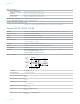
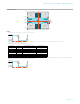
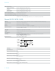
Digital I/O Interface (Not available on Model 2604B)
+5VDC
5.1kΩ
100Ω
Solid State
Fuse
Read by
firmware
Written by
firmware
+5V Pins
(on DIGITAL I/O
connector)
Digital I/O Pi n
(on DIGITAL I/O
connector)
GND Pin
(on DIGITAL I/O
connector)
Rear Panel
Connector 25-pin female D.
Input/Output Pins 14 open drain I/O bits.
Absolute Maximum Input Voltage
5.25 V.
Absolute Minimum Input Voltage
– 0.25 V.
Maximum Logic Low Input Voltage
0.7 V, +850 µA max.
Minimum Logic High Input Voltage
2.1 V, +570 µA.
Maximum Source Current (flowing out of Digital I/O bit)
+960 µA.
Maximum Sink Current @ Maximum Logic Low Voltage (0.7V)
–5.0 mA.