
User's Manual

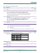


Table Of Contents
- 1. Introduction
- The PN7150 architecture overview
- 2. NCI Overview
- 3. DH interface
- 5. Initialization & Operation configuration
- 6. Reader/Writer Mode
- 6.1 T1T, T2T, MIFARE Ultralight, MIFARE Classic and MIFARE Plus tags
- 6.1.1 Access through the [NCI] Frame RF Interface
- 6.1.2 [PN7150-NCI] extension: TAG-CMD Interface
- 6.1.3 [PN7150-NCI] extension: Payload structure of the TAG-CMD RF Interface
- 6.1.4 [PN7150-NCI] extension: REQs & RSPs rules
- 6.1.5 [PN7150-NCI] extension: List of REQs & RSPs
- 6.1.6 [PN7150-NCI] extension: raw data exchange REQs & RSPs
- 6.1.7 [PN7150-NCI] extension: T2T & MFU REQs & RSPs
- 6.1.8 [PN7150-NCI] extension: MIFARE Classic REQs & RSPs
- 6.1.9 Access through the TAG-CMD RF Interface
- 6.2 T3T tag
- 6.3 T4T & ISO-DEP Tags/Cards
- 6.3.1 Access through the Frame RF Interface
- 6.3.2 Access through the ISO-DEP RF Interface
- 6.3.3 [PN7150-NCI] extension: Presence check Command/Response
- 6.3.4 [PN7150-NCI] extension: S-Block Command/Response
- 6.3.5 [PN7150-NCI] extension: WTX notification
- 6.3.6 [PN7150-NCI] extension: Higher bit rates in Poll NFC-A & NFC-B
- 6.4 [PN7150-NCI] extension: 15693 & I-Code tags
- 6.5 [PN7150-NCI] extension: KOVIO tags
- 6.1 T1T, T2T, MIFARE Ultralight, MIFARE Classic and MIFARE Plus tags
- 7. Card Emulation Mode
- 8. P2P Initiator & Target Mode
- 9. RF Discovery Management
- 9.1 RF Discovery functionalities
- 9.2 NFC FORUM Profile as defined in [NCI]
- 9.3 [PN7150-NCI] extension: additional technologies not yet supported by the NFC FORUM
- 9.4 [PN7150-NCI] extension: Low Power Card Detector (LPCD) Mode
- 9.5 [PN7150-NCI] extension: EMVCo Profile in Poll & Listen Modes
- 9.6 [PN7150-NCI] extension: Power optimization
- 10. Configurations
- 11. Test Mode
- 12. PN7150 Practical approach

U
M10936
P
N7150 User Manual
UM
10936 All information provided in this document is subject to legal disclaimers.
U
ser manual
CO
MPANY PUBLIC
Rev. 2.0 — 6 November 2020
348120
88 of 127
Na
me & Rights
D
escription
Ex
t. Tag
L
en.
D
efault
Value
P
MU_CFG
RW in E²PROM
Configuration of the Power Management Unit (PMU)
Byte 0:
Bit Mask Description
b7 b6 b5 b4 b3 b2 b1 b0
X VBAT1 connected to 5V
0 - CFG1, 1 - CFG2
0 0 0 0 0 1 0 RF
U
Byte 1:
Bit Mask Description
b7 b6 b5 b4 b3 b2 b1 b0
X
T
VDD monitoring
threshold:
0 - 3.6V (CFG1, CFG2)
1 - 5V (CFG2)
X X X T
xLDO Voltage in card
mode communication:
000: 3V (CFG1, CFG2)
001: 3.3V (CFG1, CFG2)
010: 3.6V (CFG1, CFG2)
011: 4.5V (CFG2)
100: 4.7V (CFG2)
X X X T
xLDO Voltage in reader
mode communication:
000: 3V (CFG1, CFG2)
001: 3.3V (CFG1, CFG2)
010: 3.6V (CFG1, CFG2)
011: 4.5V (CFG2)
100: 4.7V (CFG2)
0 RFU
B
yte 2: RFU. Must be 0x00 for CFG1 and 0x01 in CFG2.
0xA0 0x0E 3 0x020900
(CFG1)
D
H_EEPROM_AREA_2
RW in E²PROM
32-Byte EEPROM area dedicated to the DH to store/retrieve
non-volatile data. The 32 Bytes have to be read
(CORE_GET_CONFIG_CMD) or written
(CORE_SET_CONFIG_CMD) is a row: it is not possible to
access only a subset of these 32 Bytes.
0xA0 0x14
32
DYN_LMA_SETTINGS_
CFG
RW in E²PROM
Parameter used to Read/write the Configuration as well as
the Lookup table for the dynamic LMA feature
0xA0 0x92 68
See
Table
84