
User's Manual

Rev0.0
Page5of
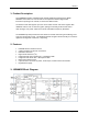
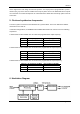
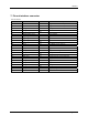
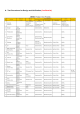
7. Pin out interface connector
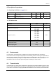
Pin information.
Pin Numbe
r
Pin Name I/O Description
1 5V
PWR
Regulated 4.7V to 5.2V input
2 5V
PWR
Regulated 4.7V to 5.2V input
3 GPIO_2
I/O
PWM_RST#
4 GPIO_13
I/O
MUTE
5 GPIO_14
I/O
POWER_CTL
6 /RESET(DARR_RST)
I
Reset Darr83
7 I
2
C_SCL_SLV
I/O
I
2
C serial clock Slave
8 I
2
C_SDA_SLV
I/O
I
2
C serial data Slave
9 I
2
C_SCL_MST
I/O
I
2
C serial clock Master
10 I
2
C_SDA_MST
I/O
I
2
C serial data Master
11 MCLK
I/O
12.288MHz audio clock I/O
12 GND
GND
GND
13 BCK_W
I/O
I
2
S port W Bit Clock
14 LRCK_W
I/O
I
2
S port W Left Right Clock
15 GPIO_5
I/O
DAT_W
16 GPIO_11
I/O
DAT_X
17 MON_TXD
I/O
Serial sync Data, for test purposes
18 GIPO_6
I/O
FW_SEL
19 GPIO_12
I/O
IR_RST#
20 GPIO_3
I/O
ID_SET#
21 GPIO_15
I/O
RED_LED
22 GPIO_4
I/O
BLUE_LED (UART_RXD)
23 GPIO_7
I/O
IR_SD#(HW_MUTE)
24 GND
GND
GND
9