
User's Manual

DOC No: ZB7412-00A-DTS-R03
____________________________________________________________________________________
Copyright © JORJIN TECHNOLOGIES INC. 2017 11
http://WWW.JORJIN.COM.TW
4. MODULE SPECIFICATIONS
4.1. Absolute Maximum Ratings
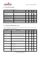
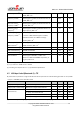
(1)(2)
over operating free-air temperature range (unless otherwise noted)
(1) All voltage values are with respect to ground, unless otherwise noted.
(2) Stresses beyond those listed under Absolute Maximum Ratings may cause permanent damage to the device. These
are stress ratings only, and functional operation of the device at these or any other conditions beyond those
indicated under Recommended Operating Conditions is not implied. Exposure to absolute-maximum-rated
conditions for extended periods may affect device reliability.
(3) VDDS2 must be at the same potential as VDDS.
(4) Including analog capable DIO.
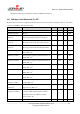
4.2. ESD Ratings
(1) JEDEC document JEP155 states that 500-V HBM allows safe manufacturing with a standard ESD control process.
(2) JEDEC document JEP157 states that 250-V CDM allows safe manufacturing with a standard ESD control process.
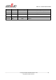
Parameter
Conditions
MIN
MAX
Unit
Supply voltage, VDDS
(3)
-0.3
4.1
V
Voltage on any digital pin
(4)
-0.3
VDDS+0.3
Max 4.1
V
Voltage on ADC input (V
in
)
Voltage scaling enabled
-0.3
VDDS
V
Internal reference, voltage scaling disabled
-0.3
1.49
V
VDDS as reference, voltage scaling disabled
-0.3
VDDS/2.9
V
Input RF level
+5
dBm
Storage temperature range
-40
+85
°C
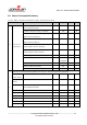
Parameter
Value
Unit
Electrostatic
discharge
performance (V
ESD
)
Human Body Model (HBM), per ANSI/ESDA/JEDEC
JS001
(1)
All pins
±2500
V
Charged Device Model (CDM), per JESD22-C101
(2)
RF pins
±750
V
Non-RF pins
±750
V