
User's Manual
Doc No: WG1400-00-DTS-D05
Copyright
©
JORJIN TECHNOLOGIES INC. 2015
http://WWW.JORJIN.COM.TW
CONFIDENTIAL
Page 11
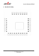
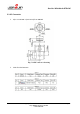
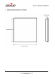
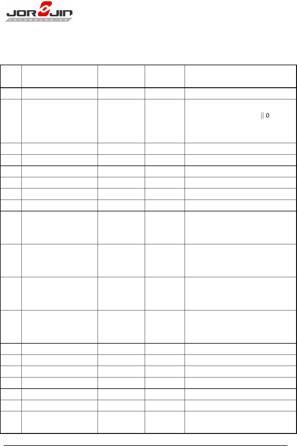
5.1. Pin Description
Pin
No.
Signal Name State at
Reset
Type Description
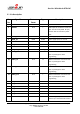
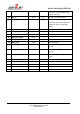
1 GND GND GND
Ground.
2 nRESET HI-Z I
RESET input for the device. Active low
input. The RC circuit (100K
∥
0.1μF)
has been built in internal for power
reset.
3 VBAT_IN POW POW
Power supply input, 2.1 to 3.6V.
4 VBAT_IN POW POW
Power supply input, 2.1 to 3.6V.
5 GND GND GND
Ground.
6 NC_06 HI-Z NA
Unused. Leave unconnected.
7 GND GND GND
Ground.
8 EXT_RTC_IN HI-Z Analog
32.768-KHz / External clock input.
9 UART_RTS HI-Z O
UART host interface. Connect to test
point on prototype for flash
programming.
10 UART_TX HI-Z O
UART host interface. Connect to test
point on prototype for flash
programming.
11 UART_RX HI-Z I
UART host interface. Connect to test
point on prototype for flash
programming.
12 UART_CTS HI-Z I
UART host interface. Connect to test
point on prototype for flash
programming.
13 NC_13 HI-Z NA
Unused. Leave unconnected.
14 NC_14 HI-Z NA
Unused. Leave unconnected.
15 NC_15 HI-Z NA
Unused. Leave unconnected.
16 NC_16 HI-Z NA
Unused. Leave unconnected.
17 NC_17 HI-Z NA
Unused. Leave unconnected.
18 NC_18 HI-Z NA
Unused. Leave unconnected.
19 HIBERNATE HI-Z I
Hibernate signal input to the NWP
(active low). If the Hibernate function