
User's Manual

Doc No: WG1300BE00 EM Board-UG-R02
Copyright © JORJIN TECHNOLOGIES INC. 2014
http://WWW.JORJIN.COM.TW
CONFIDENTIAL
Page 19
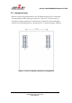
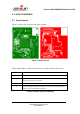
Figure 10. Module Layout Guidelines
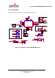
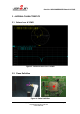
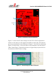
Figure 11 shows the RF trace design for the PCB. A 50-Ω impedance
match on the trace to the antenna should be used. Also, 50-Ω traces
are recommended for the PCB layout. Figure 11 also lists the distances.
Figure 12 shows layer 1 with the trace to the antenna over the layer 2.
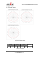
Table 9 and Figure 13 describe instances of good layout practices for
the antenna and RF trace routing.
Figure 11. Trace Design for the PCB layout
1
2, 3
4